

Semiconductor led, opto-electronic integrated circuits (OEIC), and method of fabricating oeic
a technology of optoelectronic integrated circuit and semiconductor, which is applied in the direction of semiconductor devices, solid-state devices, optical waveguide light guides, etc., can solve the problem that no silicon light emitting diode has been obtained, and achieves high luminescence efficiency and high efficiency
- Summary
- Abstract
- Description
- Claims
- Application Information
AI Technical Summary
Benefits of technology
Problems solved by technology
Method used
Image

Examples
embodiment 1
[0122]FIG. 11 is a planar layout for an integrated light emitting diode according to the present invention; FIG. 12 is a planar layout for a light receiving element according to the present invention; and FIGS. 13 through 18 are schematic cross-sectional views for stepwisely explaining the fabricating process of the integrated light emitting diode. In each of the drawings, a cross-sectional view taken along line A-A′ of the planar layout (FIG. 11) is shown on the left hand side, and a cross-sectional view taken along line B-B′ of the planar layout (FIG. 11) is shown on the right hand side.
[0123]A 1 μm thick silicon oxide film 1900 is formed on a silicon support substrate 1100 and an SOI wafer having a 100 nm thick single crystalline silicon layer 1120 is thermally oxidized on the silicon oxide film, to form a 20 nm oxide film (FIG. 13). A silicon thin film formation region (fin) and a contact region are formed (FIG. 14) by using an active region pattern 1150 shown in FIG. 11. Herein...
embodiment 2
[0137]In this embodiment, a plurality of fins are employed as an integrated light emitting diode. The fins can be formed, independently of the patterning. A so-called spacer process is employed as follows. FIG. 43 shows an exemplary planar layout, and FIGS. 45 through 60 stepwisely show the fabricating process by using cross-sectional views (A-A′ cross section of FIG. 43). This method is based on a dummy pattern 1152, but the dummy pattern can be arranged in two different forms, i.e., a convex pattern or a hole pattern. FIG. 43 shows a convex pattern, and FIG. 44 shows a hole pattern. According to the fabricating process of this embodiment, after the dummy pattern 1152 of FIG. 43 and FIG. 44 is formed, fins are self-aligned with respect to the dummy pattern. In general, because of the self-alignment, spacers 1202, 1203, 1204, 1205, 1981, 1982, and 1983 used for fin formation are not necessarily found in a photo mask, but they are indicated at pattern positions of the layout after th...
embodiment 3
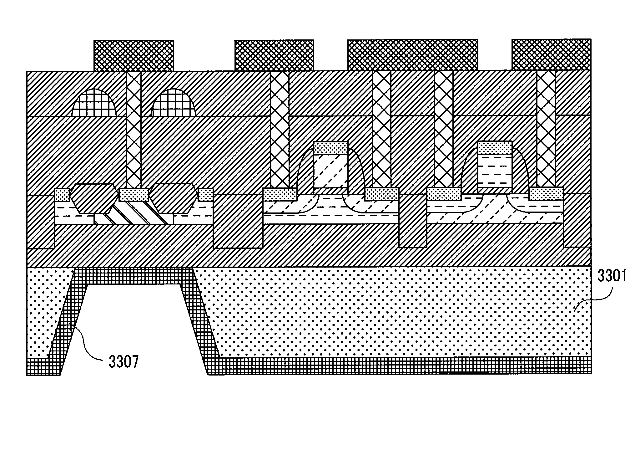
[0165]This embodiment discloses a luminous region expansion method that does not require a laminate film or plural wall-type silicon thin films disclosed in Embodiment 1 and Embodiment 2. In a light emitting diode according to this embodiment, as shown in FIG. 69, silicon semiconductor regions 3303 and 3304 of different conductive types are arranged adjacent each other on a silicon oxide film 3302 formed on the surface of the silicon substrate 3301, and a silicon oxide film 3305 is formed in the periphery of the interface of these two semiconductor regions only in such a manner that it covers a portion of the surfaces of the two semiconductor regions. Meanwhile, a silicide 3306, the compound of silicon and a metal, is formed on the surface of a semiconductor region that is not covered with the silicon oxide film 3305. In addition, a part of the silicon substrate 3301, that is, the silicon substrate in a region having the light emitting diode formed thereon, is removed to expose the ...
PUM
 Abstract
Description
Claims
Application Information