Electrolytic Copper Plating Method, Phosphorous Copper Anode for Electrolytic Copper Plating, and Semiconductor Wafer having Low Particle Adhesion Plated with said Method and Anode

a technology of electrolytic copper and copper plating, which is applied in the direction of electrolysis components, coatings, electrolysis processes, etc., can solve the problems of inferior plating, additives within the plating liquid decomposing, and new problems, and achieve the effect of preventing particle adhesion and low particle adhesion

Inactive Publication Date: 2008-09-04
JX NIPPON MINING & METALS CORP
View PDF16 Cites 8 Cited by
  • Summary
  • Abstract
  • Description
  • Claims
  • Application Information

AI Technical Summary

Benefits of technology

[0010]In order to achieve the foregoing object, as a result of intense study, the present inventors discovered that it is possible to stably perform electrolytic copper plating to the likes of a semiconductor wafer having low particle adhesion by improving the electrode materials.

Problems solved by technology

Nevertheless, when employing this electrolytic copper plate for forming copper wiring of semiconductors, a new problem arose which was not found in a PWB.
This is because when an insoluble anode formed from the likes of platinum, titanium, or iridium oxide is used, the additive within the plating liquid would decompose upon being affected by anodic oxidization, and inferior plating will occur thereby.
Moreover, when employing electrolytic copper or oxygen-free copper of a soluble anode, a large amount of particles such as sludge is generated from metallic copper or copper oxide caused by the disproportionation reaction of monovalent copper during dissolution, and the plating object will become contaminated as a result thereof.
Nevertheless, even upon employing phosphorous copper as the anode as described above, it is not possible to completely control the generation of particles since metallic copper or copper oxide is produced where the black film drops off or at portions where the black film is thin.
Nevertheless, when this kind of method is employed, particularly in the plating of a semiconductor wafer, there is a problem in that minute particles, which were not a problem in forming the wiring of a PWB and the like, reach the semiconductor wafer, such particles adhere to the semiconductor, and thereby cause inferior plating.

Method used


Image

  • Electrolytic Copper Plating Method, Phosphorous Copper Anode for Electrolytic Copper Plating, and Semiconductor Wafer having Low Particle Adhesion Plated with said Method and Anode
  • Electrolytic Copper Plating Method, Phosphorous Copper Anode for Electrolytic Copper Plating, and Semiconductor Wafer having Low Particle Adhesion Plated with said Method and Anode

Examples


examples 1 to 3

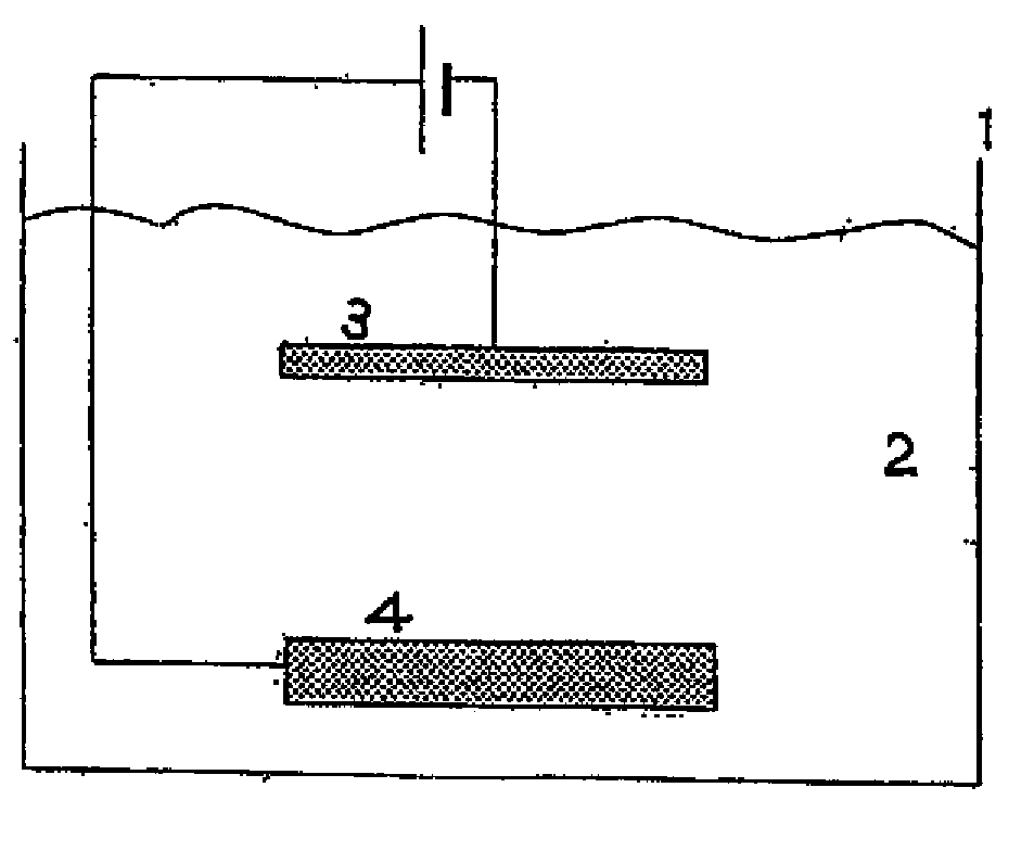
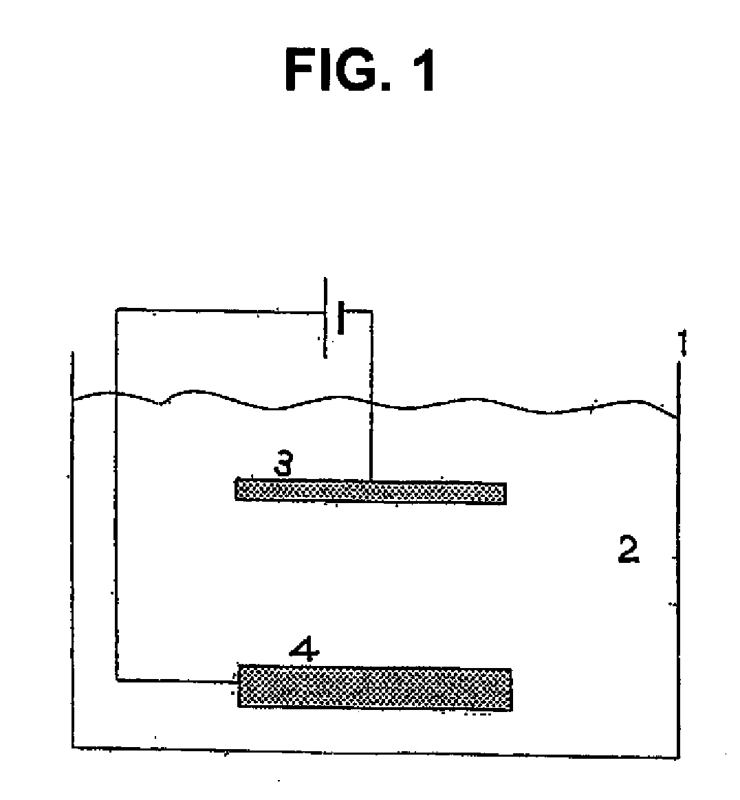
[0037]As shown in Table 1, phosphorous copper having a phosphorous content of 500 wtppm was used as the anode, and a semiconductor wafer was used as the cathode. The crystal grain size of these phosphorous copper anodes was 1,800 μm, 5,000 μm and 18,000 μm.

[0038]As the plating liquid, copper sulfate: 20 g / L (Cu), sulfuric acid: 200 g / L, chlorine ion 60 mg / L, additive [brightening agent, surface active agent] (Product Name CC-1220: manufactured by Nikko Metal Plating): 1 mL / L were used. The purity of the copper sulfate in the plating liquid was 99.99%.

[0039]The plating conditions were plating temperature 30° C., cathode current density 3.0 A / dm2, anode current density 3.0 A / dm2, and plating time 120 hr.

[0040]The foregoing conditions are shown in Table 1.

[0041]After the plating, the generation of particles and plate appearance were observed. The results are similarly shown in Table 1. Regarding the number of particles, after having performed electrolysis under the foregoing electrolyt...


PUM

PropertyMeasurementUnit
crystal grain sizeaaaaaaaaaa

Abstract

An electrolytic copper plating method characterized in employing a phosphorous copper anode having a crystal grain size of 1,500 μm (or more) to 20,000 μm in an electrolytic copper plating method employing a phosphorous copper anode. Upon performing electrolytic copper plating, an object is to provide an electrolytic copper plating method of a semiconductor wafer for preventing the adhesion of particles, which arise at the anode side in the plating bath, to the plating object such as a semiconductor wafer, a phosphorous copper anode for electrolytic copper plating, and a semiconductor wafer having low particle adhesion plated with such method and anode.

Description

CROSS REFERENCE TO RELATED APPLICATIONS[0001]This application is a continuation of co-pending U.S. application Ser. No. 10 / 478,750, which is the National Stage of International Application No. PCT / JP02 / 12437, filed Nov. 28, 2002, which claims the benefit under 35 USC 119 of Japanese Application No. 2002-074659, filed Mar. 18, 2002.BACKGROUND OF THE INVENTION[0002]The present invention pertains to an electrolytic copper plating method capable of preventing the adhesion of particles to a plating object, a semiconductor wafer in particular, a phosphorous copper anode for such electrolytic copper plating, and a semiconductor wafer having low particle adhesion and electrolytic copper plated with the foregoing method and anode.[0003]Generally, although an electrolytic copper plate has been employed for forming copper wiring in a PWB (print wiring board) or the like, in recent years, it is being used for forming copper wiring of semiconductors. An electrolytic copper plate has a long histo...

Claims


Application Information

Patent Timeline
Patent Type & Authority Applications(United States)
IPC IPC(8): C25D3/00C25D17/10C25D3/38C25D7/12H01L21/288
CPCC25D3/38C25D17/10C25D7/12C25D21/12
Inventor AIBA, AKIHIROOKABE, TAKEO
Owner JX NIPPON MINING & METALS CORP
Why Eureka
Try Eureka