Method for manufacturing patterned vapor-deposited film

Inactive Publication Date: 2008-09-18
FUJI ELECTRIC HLDG CO LTD
View PDF10 Cites 8 Cited by
  • Summary
  • Abstract
  • Description
  • Claims
  • Application Information

AI Technical Summary

Benefits of technology

[0022]With the configuration in accordance with the present invention, a patterned vapor-deposited film can be formed by heating only the selected heating elements of the deposition panel in a state in which they face the device panel and selectively evaporating the deposition material located on the selected heating elements. With the method in accordance with the present invention, a pattern of desired high resolution can be easily formed because no metal mask is used. Further, because no laser scanning device is used, a patterned vapor-deposited film can be formed inexpensively and within a short time.
[0023]In addition, because only the deposition material in a n

Problems solved by technology

However, because patterning of the obtained color conversion layer after it has been formed is difficult, separate light emission of three primary colors is impossible.
The following problems are associated with the above-described conventional methods for forming fine patterns of thin films of deposition materials.
First, material and thickness of a metal mask causes limitation on size reduction of a mask pattern.
The problem is that the manufacturing process becomes more difficult and yield drops in the manufacture of patterns with higher resoluti

Method used


Image

  • Method for manufacturing patterned vapor-deposited film
  • Method for manufacturing patterned vapor-deposited film
  • Method for manufacturing patterned vapor-deposited film

Examples


example 1

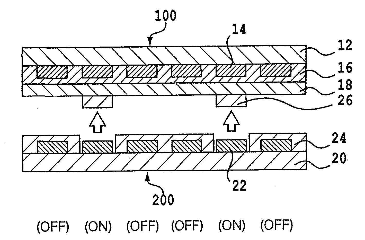
[0059]A TFT substrate 12 in which a plurality of switching elements composed of TFT were arranged with a pitch of 42 μm in the X direction and a pitch 126 μm in the Y direction on a silicon substrate was disposed inside a DC sputtering apparatus. A CrB film having a thickness of 100 nm and an IZO (In2O3—10% ZnO) film having a thickness of 20 nm were formed using a DC sputtering method in which a 300 W sputtering power was applied in an Ar atmosphere. The laminate of the CrB film and IZO film thus obtained was patterned, and a plurality of partial electrodes having dimensions of 32 μm in the X direction and 116 μm in the Y direction are formed for reflecting electrodes 14 arranged with a pitch of 42 μm in the X direction and 126 μm in the Y direction.

[0060]The TFT substrate 12 with the reflecting electrodes 14 formed thereon was transferred into a vapor deposition apparatus, and an organic EL layer 16 was formed. During film formation, the internal pressure in the vacuum chamber was ...

example 2

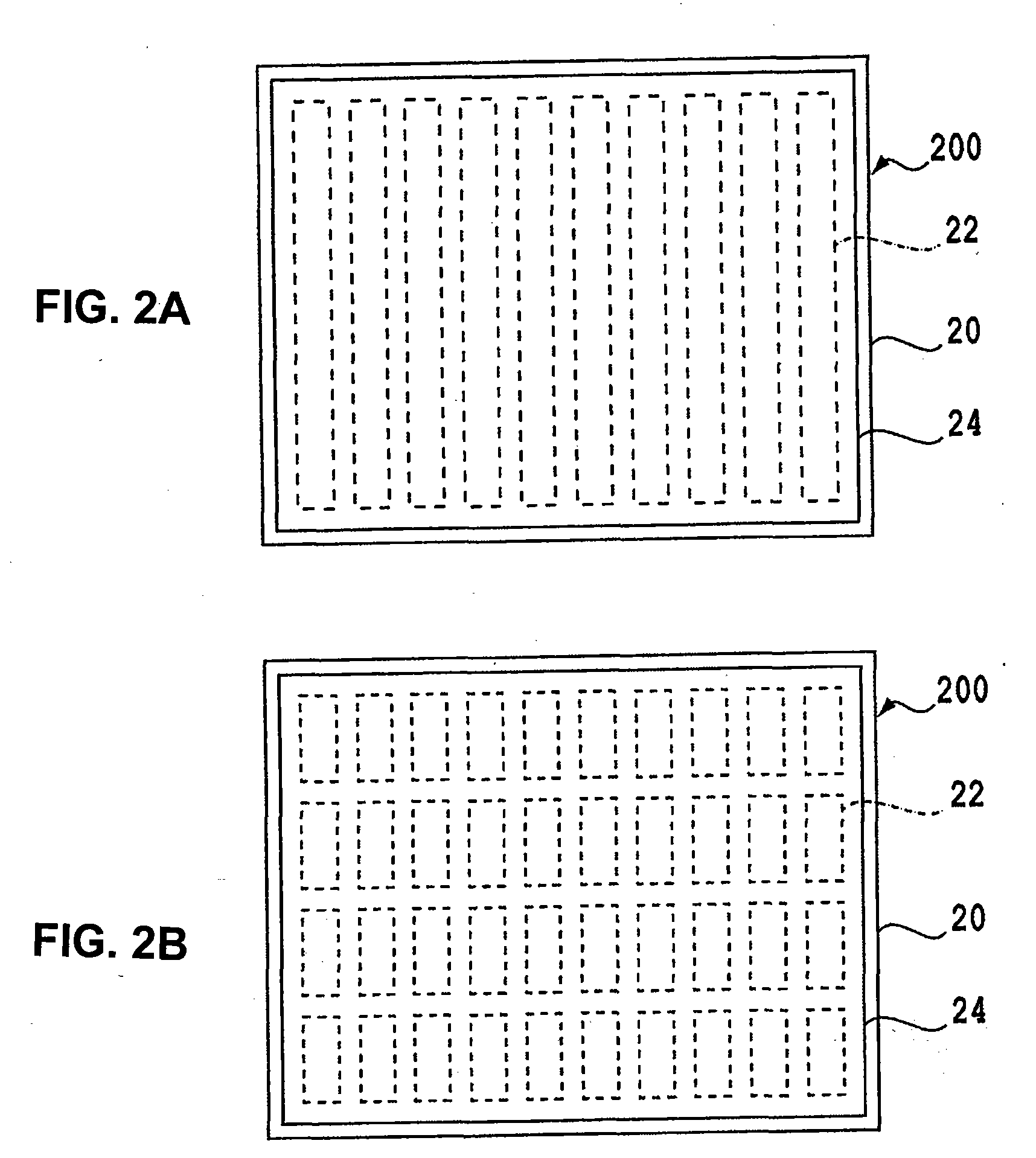
[0065]An Al film having a thickness of 1 μm was formed using a sputtering method on a quartz substrate 20 having a thickness of 5 mm. Then, a plurality of X wirings 38 were formed by a photolithography method using the usual wet etching process. Each of a plurality of X wirings 38 had a trunk portion extending in the X direction and a plurality of branches that were branched out from the trunk and extended in the Y direction. Trunk portions of the X wirings 38 were arranged with a pitch of 42 μm in the Y direction. Further, the branches of X wirings 38 had a linear shape with a length of 24 μm that extended in the Y direction; the branches were arranged with a pitch of 42 μm in the X direction. The trunks and branches of the X wirings had a width of 10 μm.

[0066]A SiOx film having a thickness of 300 μm was deposited by a sputtering method so as to cover the X wirings 38. Then, an insulating film 34 was obtained by forming contact holes 36 by RIE using CF4 gas so as to expose the bran...


PUM

PropertyMeasurementUnit
Transparencyaaaaaaaaaa
Resolution enthalpyaaaaaaaaaa

Abstract

A method for manufacturing a vapor-deposited film having a high-resolution pattern, without using a metal mask that makes it difficult to realize high resolution or an expensive laser scanning device. A patterned vapor-deposited film is manufactured by a method including: preparing a deposition panel containing a substrate, a plurality of heating elements, and a deposition material layer formed on the plurality of heating elements, the deposition material layer forming the outermost surface; disposing the deposition panel and a device substrate so that the deposition material layer faces the device substrate; and causing at least some of the plurality of heating elements to generate heat, selectively evaporating the deposition material layer that is positioned on the heating elements that have generated heat, and vapor depositing on a surface of the device substrate to form a vapor-deposited film.

Description

BACKGROUND[0001]The present invention relates to a method for forming a patterned vapor-deposited film. More specifically, the present invention relates to a method for manufacturing an organic EL display panel in which at least one color from among three primary colors is emitted by a color conversion layer formed according to the shape of pixels by using the method for forming a patterned vapor-deposited film.[0002]Research on practical applications of organic EL elements have been actively conducted in recent years. Organic EL elements are expected to realize a high emission brightness and emission efficiency because they can realize a high current density under a low voltage. In particular, practical applications of organic multicolor EL display panels that enable high-resolution multicolor or full-color display are expected. One of the methods for realizing multicolor or full-color organic EL display panels uses a plurality of color filters that transmit light within a specific...

Claims


Application Information

Patent Timeline
IPC IPC(8): B05D5/12
CPCC23C14/04C23C14/12H01L51/0013H01L27/322H01L27/3241C23C14/243Y02E10/549Y02P70/50H10K59/10H10K59/38H10K71/18H10K71/166H10K77/10H10K50/11B05D5/12
Inventor KAWAMURA, YUKINORIMAKINO, RYOHEIKAWAGUCHI, KOJI
Owner FUJI ELECTRIC HLDG CO LTD
Why Eureka
Try Eureka