

Group III Nitride Semiconductor Multilayer Structure
a semiconductor and multi-layer technology, applied in semiconductor/solid-state device manufacturing, semiconductor devices, electrical devices, etc., can solve the problems of large lattice mismatch, difficulty in employing, and difficult growth of iii nitride single crystals, and achieve excellent crystallinity, excellent crystallinity, and smooth surface
- Summary
- Abstract
- Description
- Claims
- Application Information
AI Technical Summary
Benefits of technology
Problems solved by technology
Method used
Image

Examples
example 1
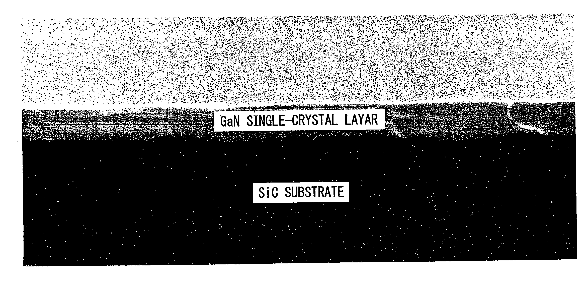
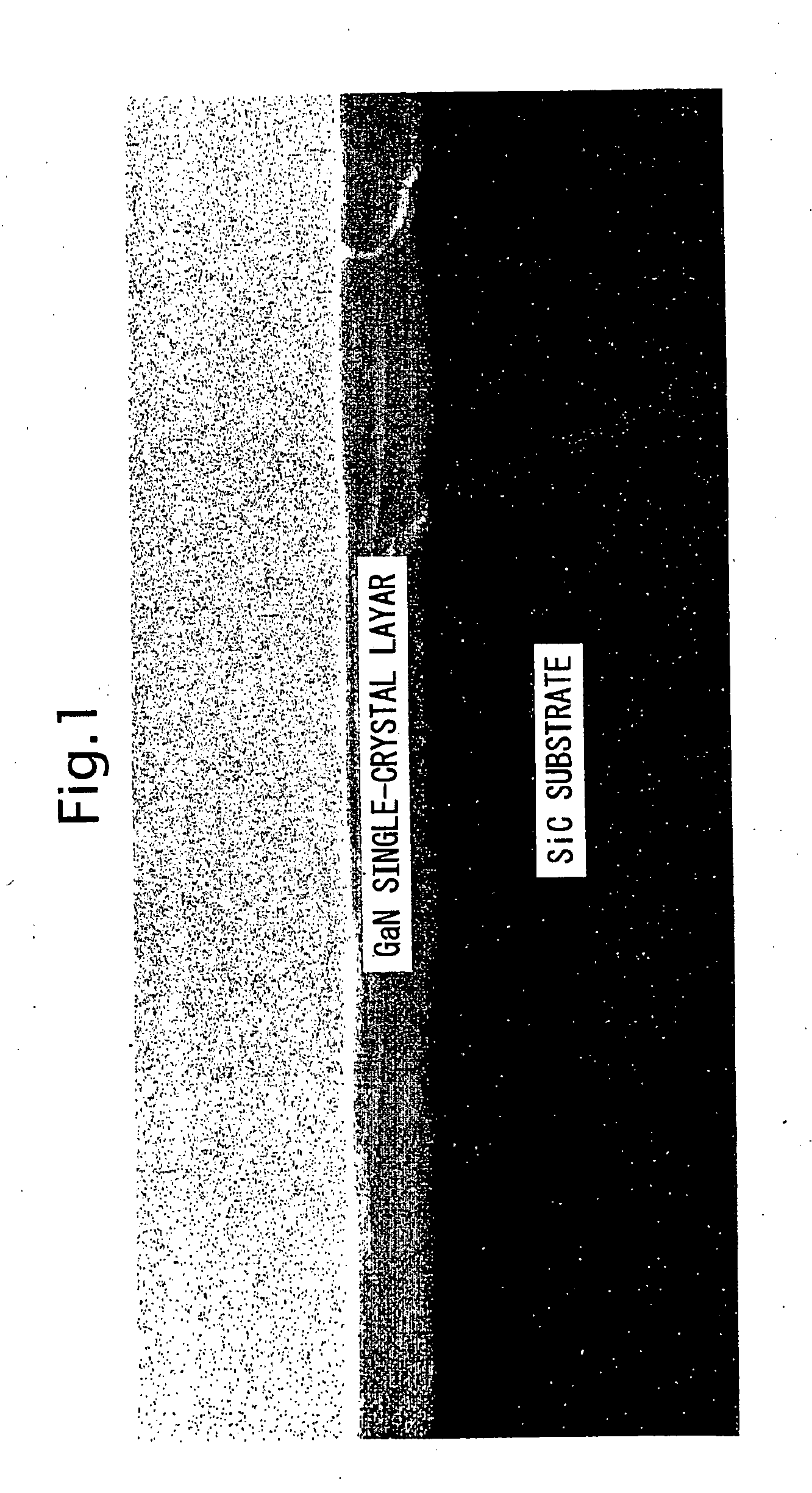
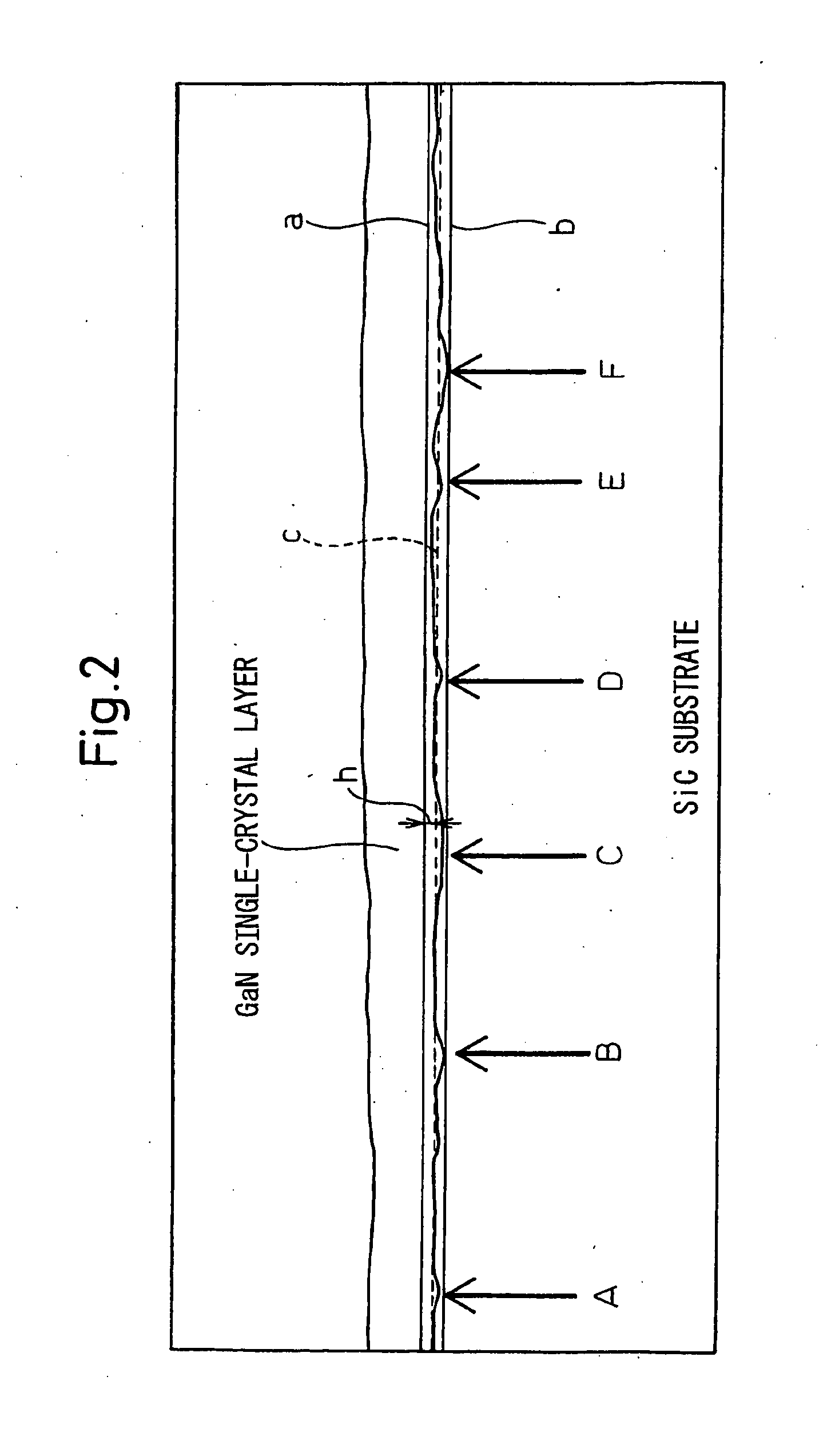
[0063]A plate-like SiC single crystal substrate having a thickness of 450 μm was cut out of an n-SiC ingot through batch slicing by use of a #400 electrodeposited wire saw. During the course of slicing, non-periodically distributed grooves (scratches) (density: several to 10 grooves / 0.1 mm) were formed on the cut surface of the substrate. The depth of the deepest groove was found to be about 1 μm; i.e., the average depth of the grooves was found to be about 0.5 μm.
[0064]After the substrate was washed with acetone, the substrate was subjected to surface etching treatment by use of a dry etching apparatus, so as to remove a process-affected layer from the substrate. Specifically, the substrate was subjected to five-minute etching treatment by use of chlorine-containing gas under the following conditions: RF power: 1 kW, bias power: 300 W. The average etching depth was regulated to 2 μm. The non-periodically distributed grooves were observed to remain on the substrate even after the et...
example 2
[0071]The procedure of Example 1 was repeated, except that the temperature for growth of a GaN single-crystal layer was regulated to 1,000° C., to thereby produce a Group III nitride semiconductor multilayer structure. The thus-produced semiconductor multilayer structure exhibited satisfactory smoothness, although a small amount of pits remained on the surface of the multilayer structure, and the surface roughness (Ra) of the multilayer structure was found to be 100 nm, which is high when compared with the case of the semiconductor multilayer structure of Example 1.
example 3
[0072]By use of the Group III nitride semiconductor multilayer structure of Example 1, a GaN-type light-emitting device which emits light having a wavelength of 460 nm was produced by means of a method known in the art.
[0073]Specifically, after growth of the GaN single-crystal layer in Example 1, an n-type layer formed of a silicon-doped GaN layer (carrier concentration: 1×10¹⁹ / cm3) was laminated by use of SiH4 serving as a dopant. Thereafter, the substrate temperature was lowered to 750° C., and an MQW light-emitting layer formed of five layer units, each including an In0.16Ga0.84N layer (thickness: 3 nm) and a GaN layer (thickness: 7 nm), was laminated. Subsequently, the substrate temperature was elevated again, and a p-type layer (thickness: 100 nm) formed of a magnesium-doped GaN layer was laminated.
[0074]Subsequently, a portion of the p-type layer and a portion of the light-emitting layer were removed through typical photolithography and dry etching techniques, to thereby expos...
PUM
| Property | Measurement | Unit |
|---|---|---|
| depth | aaaaa | aaaaa |
| depth | aaaaa | aaaaa |
| thickness | aaaaa | aaaaa |
Abstract
Description
Claims
Application Information