Unlock instant, AI-driven research and patent intelligence for your innovation.
Semiconductor Device and Method for Fabricating the Same
Inactive Publication Date: 2008-10-23
SILICONWARE PRECISION IND CO LTD
View PDF9 Cites 11 Cited by
Summary
Abstract
Description
Claims
Application Information
AI Technical Summary
This helps you quickly interpret patents by identifying the three key elements:
Problems solved by technology
Method used
Benefits of technology
Benefits of technology
[0012]In view of the aforementioned drawbacks, it is an objective of the present invention to provide a semiconductor device and a method for fabricating the same, which can integrate more chips in the semiconductor device without increasing the die attachment area.
[0013]It is another objective of the present invention to provide a semiconductor device and a method for fabricating the same, allowing the semiconductor device to be more simply fabricated, thereby avoiding complex processes and increased cost caused by multiple applications of sputtering.
[0014]It is still another objective of the present invention to provide a semiconductor device and a method for fabricating the same, allowing a plurality of semiconductor chips to be vertically stacked and electrically connected to each other, thereby avoiding poor electrical connection caused by wire-bonding technique.
Problems solved by technology
The aforementioned conventional multi-chip semiconductor packages has a critical drawback that the chips mounted on the substrate must be spaced apart from each other to avoid interference or undesirable contact between the bonding wires for the respective chips.
This undoubtedly causes cost increase and also is not favorable for profile miniaturization of the semiconductor package.
Although the vertical chip-stacking arrangement of this semiconductor package is more spatially efficient than the horizontal chip arrangement of the above multi-chip semiconductor package, the need of bonding wires for electrical connection between the chips and the substrate makes such electrical connection susceptible to the length of the bonding wires and become degraded.
Moreover, the offset arrangement of the vertically stacked chips and the provision of the bonding wires occupy a considerably large area on the substrate, thereby limiting the number of chips that can be mounted on the substrate.
However, this technique is very complicated and has high cost, and thus is not commonly applicable in the industry.
However, with the cutting groove provided on the non-active surface (backside) of the wafer, positional alignment is not easily made, such that subsequently formed circuits may not be accurately positioned, and may adversely affect the electrical connection between the active and non-active surfaces of the chips and even damage the chips.
Moreover, the RDL technique is applied multiple times during fabrication, thereby increasing the cost and process complexity.
Further, as the fabrication process is performed directly on the wafer, no test for verifying whether the chips are “good dies” (non-defective chips) or not is conducted in advance, such that the fabrication process continues even if the wafer contains defective chips.
This undesirably leads to material waste and increased cost.
Therefore, the problem to be solved here is to provide a semiconductor device that can effectively integrate more chips in the semiconductor device to enhance the electrical performance thereof, without increasing the die attachment area, without using bonding wires (which may cause degraded electrical connection), without using the TSV technique or multiple times of the sputtering technique (which may cause complicated processes and increased cost), and without performing the fabrication process directly on a wafer in the absence of the “good die” concern.
Method used
Image
Click on the blue label to locate the original text in one second.
Reading with bidirectional positioning of images and text.
Examples
first embodiment
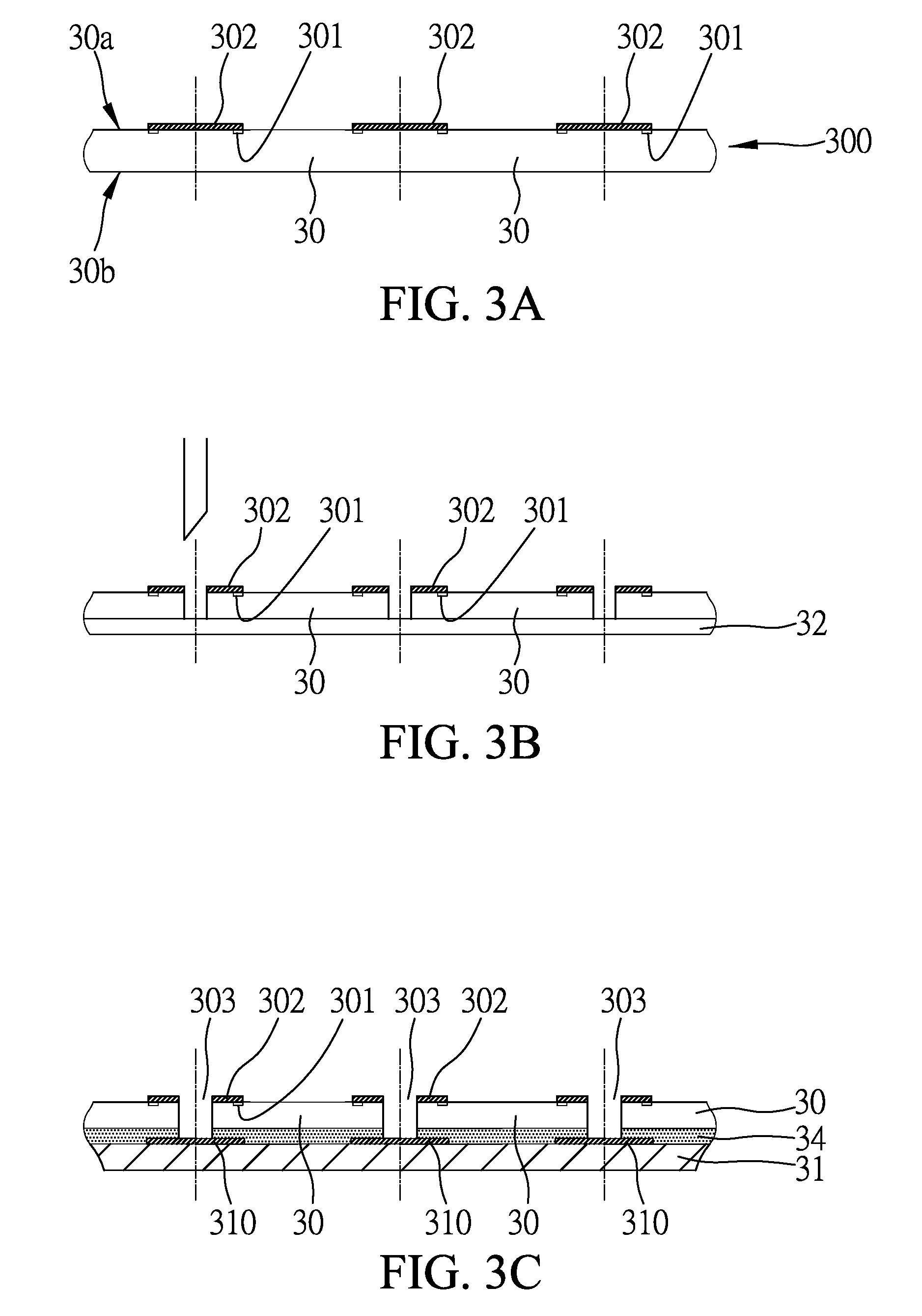
[0038]FIGS. 3A to 3G show a semiconductor device and a method for fabricating the same according to the first embodiment of the present invention.
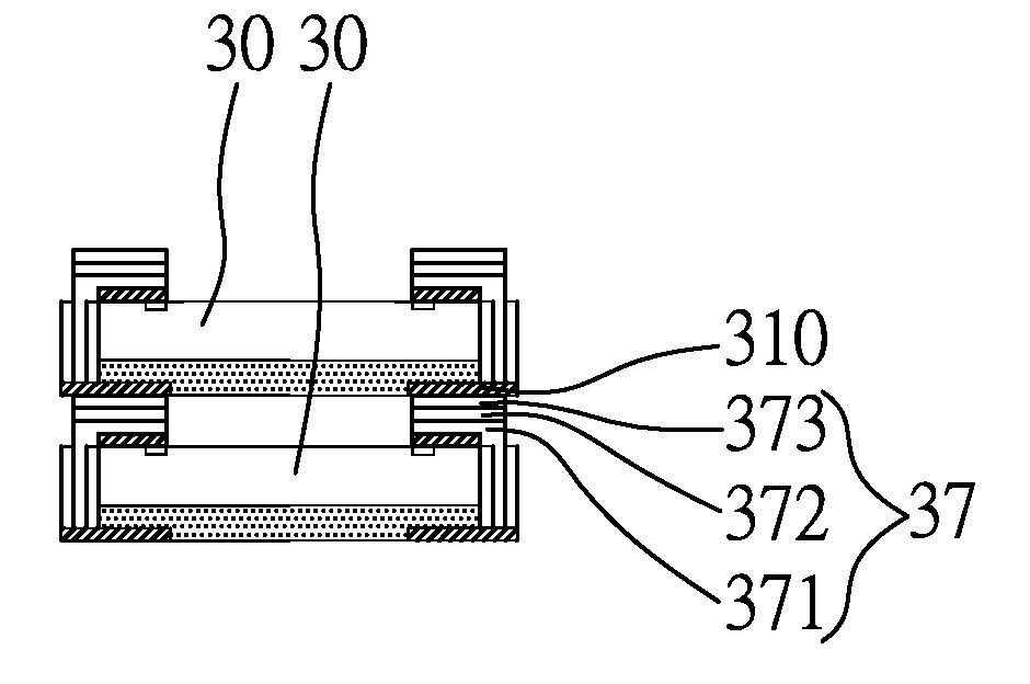
[0039]As shown in FIGS. 3A and 3B, a wafer 300 has a plurality of chips 30. Each of the chips 30 and the wafer 300 has an active surface 30a and an opposing non-active surface 30b, wherein a plurality of bond pads 301 are formed on the active surface 30a of each of the chips 30. After a chip probing (CP) process is performed on each of the chips 30 to determine that the chips are good dies (non-defective chips), a first metal layer 302 is formed on any adjacent two of the chips 30 and is electrically connected to the bond pads 301 on the adjacent chips. The first metal layer 302 is, for example, an under bump metallurgy (UBM) layer made of titanium / copper / nickel (Ti / Cu / Ni), titaniumtungsten / gold (TiW / Au), aluminum / nickelvanadium / copper (Al / NiV / Cu), titanium / nickelvanadium / copper (Ti / NiV / Cu), titanium tungsten / nickel (TiW / Ni), titanium / c...
second embodiment
[0049]FIGS. 5A and 5B show a semiconductor device and a method for fabricating the same according to a second embodiment of the present invention. For brevity, as compared with the first embodiment, identical or similar elements are denoted with identical or similar reference numerals in the second embodiment.
[0050]The semiconductor device and its fabrication method in the second embodiment are similar to those in the first embodiment. The difference resides in that, as shown in FIG. 5A, after the second metal layers 37 are formed and the resist layer is removed, an insulating layer 38 is formed over the active surface of the chips 30 and the second metal layers 37. The insulating layer 38 can be an epoxy resin layer. Next, the carrier is removed by etching, and singulation is performed along the dielectric layer 35 to separate the chips 30. Consequently, a plurality of semiconductor devices such as thin CSP devices are formed.
[0051]As shown in FIG. 5B, a plurality of conductive ele...
third embodiment
[0053]FIGS. 7A to 7E show a semiconductor device and a method for fabricating the same according to a third embodiment of the present invention. For brevity, as compared with the above embodiments, identical or similar elements are denoted with identical or similar reference numerals in the third embodiment.
[0054]The semiconductor device and its fabrication method in the second embodiment are similar to those in the above embodiments. The difference resides in that, as shown in FIG. 7A, when a plurality of first metal layers 302 are formed on the active surfaces of the chips 30 by means of the RDL technique, the first metal layers 302 can have extending portions extended through the bond pads 301 and towards the centers of the chips 30. A plurality of extension pads 304 are formed on at ends of the extending portions of the first metal layers 302.
[0055]As shown in FIG. 7B, similar to the descriptions in the above embodiments, the chips 30 are mounted on the carrier 31 having the con...
PUM
Abstract
The present invention provides a semiconductor device and a method for fabricating the same. The semiconductor device includes a chip having an active surface and an opposing non-active surface, wherein a plurality of bond pads are formed on the active surface, and first metallayers are formed on the bond pads and to edges of the non-active surface; conductive traces disposed on the non-active surface of the chip; a dielectric layer covering sides of the chip and formed with a plurality of openings therein to expose a portion of the conductive traces; and a plurality of second metallayers formed in the openings of the dielectric layer and on the first metallayers, such that the bond pads are electrically connected to the conductive traces via the first and second metal layers.
Description
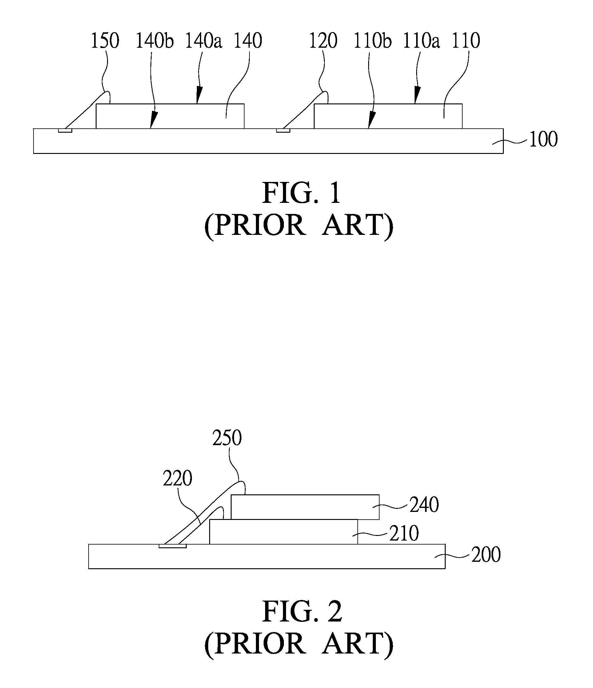
BACKGROUND OF THE INVENTION[0001]1. Field of the Invention[0002]The present invention generally relates to semiconductor devices and methods for fabricating the same, and more particularly, to a semiconductor device that can be vertically stacked on another semiconductor device, and a method for fabricating the semiconductor device.[0003]2. Description of Related Art[0004]Multi-Chip Module (MCM) is a highly integrated form of semiconductor package and is characterized in having at least two chips mounted on a carrier (such as a substrate or lead frame) in a single semiconductor package. The MCM has been widely adopted in electronic devices (such as portable electronic products and associated peripheral products for communication, network and computer fields) for its advantages of enhancing the performance and capacity of the semiconductor package, thereby suitable for the electronic devices which are being made with low profile, large capacity and high speed.[0005]FIG. 1 shows a con...
Claims
Application Information
Patent Timeline
Application Date:The date an application was filed.
Publication Date:The date a patent or application was officially published.
First Publication Date:The earliest publication date of a patent with the same application number.
Issue Date:Publication date of the patent grant document.
PCT Entry Date:The Entry date of PCT National Phase.
Estimated Expiry Date:The statutory expiry date of a patent right according to the Patent Law, and it is the longest term of protection that the patent right can achieve without the termination of the patent right due to other reasons(Term extension factor has been taken into account ).
Invalid Date:Actual expiry date is based on effective date or publication date of legal transaction data of invalid patent.

