
Photoelectric Conversion Devices

a technology of photoelectric conversion and material, applied in the field of material for photoelectric conversion devices, can solve the problems of large quantity of energy required to produce the device, inability to consider the effectiveness of solar cells using inorganic semiconductors at the present stage, and influence on the existence of humans, etc., to achieve low toxicity, easy to adapt, and good workability and productivity

Inactive Publication Date: 2008-10-30
JAPAN SCI & TECH CORP +1
View PDF4 Cites 9 Cited by
  • Summary
  • Abstract
  • Description
  • Claims
  • Application Information

AI Technical Summary

Benefits of technology

[0013]An object of the present invention is to provide materials for photoelectric conversion devices that have good workability and productivity and low toxicity, can be easily flexibilized, and have high photoelectric conversion efficiencies; and photoelectric conversion devices using said materials.

Problems solved by technology

Recently, global warming caused by burning fossil fuel and increase in energy demand associated with population growth have been serious problems influencing existence of human being.
In light of the purpose mentioned in the beginning, namely, for preventing damage to the global environment by reducing consumption of fossil fuel, however, solar cells using inorganic semiconductors cannot be regarded to be sufficiently effective at the present stage.
This is because such solar cells using inorganic semiconductors are produced by a plasma-assisted CVD method or a high-temperature crystal growth process, which means that a large quantity of energy is required to produce the devices.
Further, such devices contain Cd, As, Se or the like, which possibly have harmful effects on the environment, causing possibility of environmental damages on disposal of the devices.
While such Schottky barrier solar cells can attain relatively high open-circuit voltage (Voc), they have a drawback that the photoelectric conversion efficiencies tend to decrease with an increase in irradiation light intensity.
Further, production of Schottky barrier solar cells is generally rather difficult since thin films are required to be formed by various kinds of vapor deposition methods.
The conversion efficiencies of such pn junction solar cells are relatively high but not sufficient (see Non-patent Document 2).
In many cases, it is also required to form films by vapor deposition methods as in the case of Schottky barrier solar cells, which impedes improvement of productivity.
However, a problem was pointed out for the use of an electrolytic solution and iodine, and commercialization has been hard to progress.
Although various methods have been tried for the solidification, the photoelectric conversion efficiencies of such systems are still lower than those of wet-type solar cells using electrolytic solutions.
For example, conductive polymers such as polyaniline, polypyrrole, polythiophene, and the like, have been examined, but the conversion efficiency is low in any case (see Non-patent Document 4).
To selectively generate a crystal form in a film forming step by a vapor deposition method, improvement has been attempted by controlling the substrate temperature, but it is difficult to obtain a semiconductor layer in the desired crystal form having good photoelectric characteristics.Non-patent Document 1: R. O. Loutfy et al., J. Chem. Phys. (1979), Vol. 71, p.

Method used


Image

  • Photoelectric Conversion Devices
  • Photoelectric Conversion Devices
  • Photoelectric Conversion Devices

Examples


synthesis example 1

Synthesis of Compound 1 of the Present Invention

[0098]Compound 1 of the present invention represented by the following formula was synthesized as follows.

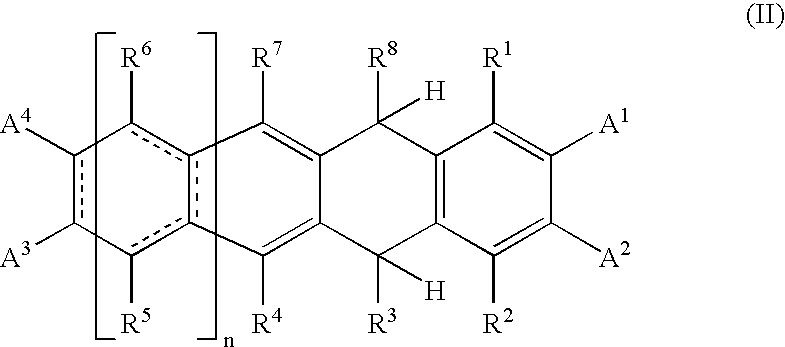
[0099]To zirconocene dichloride dissolved in THF, 2 equivalents of n-butyllithium were added at −78° C., and the resultant mixture was stirred for 1 hr. To this solution was added 1 equivalent of Diyne 1, the compound shown below, and the mixture was stirred at room temperature to generate Zirconacyclopentadiene 1, the compound shown below. To this compound were added 2 equivalents of NiCl2(PPh3)2 complex and 1 equivalent of diphenylacetylene, and the resultant mixture was stirred at 50° C. for 3 hr to obtain dihydro-compound of Compound 1, which was reacted with 1 equivalent of 2,3-dichloro-5,6-dicyanobenzoquinone (DDQ) to obtain Compound 1 as red crystals. Compound 1 obtained here was purified by sublimation and used for evaluation of the photoelectric conversion device described below.

synthesis example 2

Synthesis of Compound 2 of the Present Invention

[0100]Compound 2 of the present invention represented by the following formula was synthesized as follows.

[0101]To zirconocene dichloride dissolved in THF, 2 equivalents of n-butyllithium were added at −78° C., and the resultant mixture was stirred for 1 hr. To this solution was added 1 equivalent of Diyne 2, the compound shown below, and the mixture was stirred at room temperature to generate Zirconacyclopentadiene 2, the compound below. To this compound were added 2 equivalents of CuCl, 3 equivalents of N,N-dimethylpropyleneurea (DMPU), and 1 equivalent of dimethyl acetylenedicarboxylate (DMAD), and the resultant mixture was stirred at 50° C. for 3 hr to obtain dihydro-compound of Compound 2, which was reacted with 1 equivalent of 2,3-dichloro-5,6-dicyanobenzoquinone (DDQ) to obtain Compound 2. Compound 2 obtained here was purified by sublimation and used for evaluation of the photoelectric conversion device described below.

synthesis example 3

Synthesis of Compound 3 of the Present Invention

[0102]Compound 3 of the present invention represented by the following formula was synthesized as follows.

[0103]To zirconocene dichloride dissolved in THF, 2 equivalents of n-butyllithium were added at −78° C., and the resultant mixture was stirred for 1 hr. To this solution was added 0.5 equivalent of Tetrayne 3, the compound shown below, and the mixture was stirred at room temperature to generate Zirconacyclopentadiene 3, the compound below. To this compound were added 4 equivalents of NiCl2(PPh3)2 complex and 2 equivalents of 5-decyne, and the resultant mixture was stirred at 50° C. for 3 hr to obtain tetrahydro-compound of Compound 3, which was reacted with 2 equivalents of chloranil to obtain Compound 3. Compound 3 obtained here was purified by sublimation and used for evaluation of the photoelectric conversion device described below.


PUM

PropertyMeasurementUnit
temperatureaaaaaaaaaa

Abstract

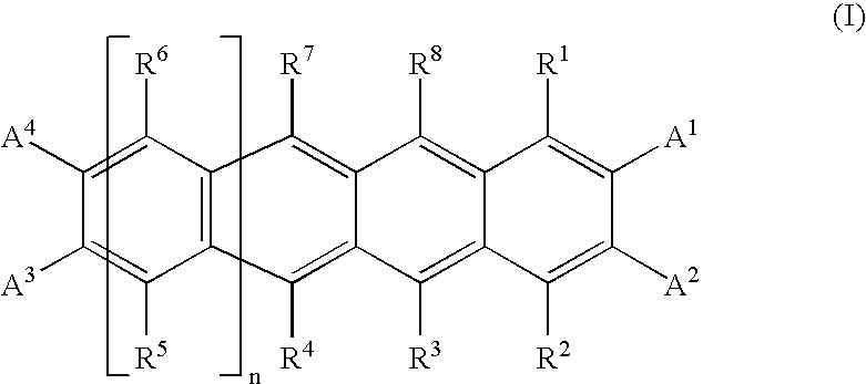
Materials for photoelectric conversion devices, consisting of polyacene derivatives represented by general formula (I) below; and photoelectric conversion devices made by using the materials. The materials for photoelectric conversion devices have excellent workability and productivity, exhibit low toxicity, are easily flexibilized, and have high photoelectric conversion efficiencies.In the formula, R1, R2, R3, R4, R5, R6, R7, R8, A1, A2, A3, and A4 are independent from each other, either the same or different, and each represents a hydrogen atom, a halogen atom, an optionally substituted hydrocarbon group having 1 to 40 carbon atoms, or the like. n is an integer of 1 or more.

Description

TECHNICAL FIELD[0001]The present invention relates to materials for photoelectric conversion devices that generate electromotive force upon photoirradiation and photoelectric conversion devices using said materials.BACKGROUND ART[0002]Recently, global warming caused by burning fossil fuel and increase in energy demand associated with population growth have been serious problems influencing existence of human being. Needless to say, sunlight has fostered terrestrial environment and supplied energy to all the living things including human being since ancient times. Thus, recently it has been considered to utilize sunlight as an energy source that is infinitely available and clean without emission of any harmful substances. In particular, attention has been paid to photoelectric devices converting light energy to electric energy, so-called solar cells, as a powerful technology.[0003]As materials for generating electromotive force in solar cells, there have been used silicon in a single...

Claims


Application Information

Patent Timeline
Patent Type & Authority Applications(United States)
IPC IPC(8): H01L31/00C07C15/20C07C15/38C07C25/22C07C69/00C07C69/76C07C255/52C07D209/58C07D487/04H01L31/04H01M14/00H10K99/00
CPCB82Y10/00C07C15/20C07C15/38C07C69/76C07C255/52C07C2103/44C07C2103/52C07D209/58C07D487/04H01L51/0046H01L51/0053H01L51/0054H01L51/0055H01L51/0059H01L51/0077H01L51/0078H01L51/4206H01L51/424Y02E10/549C07C2603/44C07C2603/52H10K85/211H10K85/623H10K85/621H10K85/622H10K85/631H10K85/311H10K85/30H10K30/451H10K30/20H10K30/50H01L31/04C07C25/22
Inventor TAKAHASHI, TAMOTSUMUSHA, KIYOSHI
Owner JAPAN SCI & TECH CORP
Learn More