Manufacturing method of SOI substrate and manufacturing method of semiconductor device

a manufacturing method and semiconductor technology, applied in semiconductor devices, basic electric elements, electrical equipment, etc., can solve the problems of difficult formation of large-area single-crystal silicon layers as described above over a substrate, and achieve the effects of preventing warpage of glass substrates and single-crystal semiconductor layers, reducing the interface state density of an interface between a single-crystal semiconductor layer and a glass substrate, and high performan

Inactive Publication Date: 2008-11-13
SEMICON ENERGY LAB CO LTD
View PDF13 Cites 24 Cited by
  • Summary
  • Abstract
  • Description
  • Claims
  • Application Information

AI Technical Summary

Benefits of technology

[0025]Shrink of a glass substrate due to heat treatment is utilized so that a distance between single-crystal semiconductor layers, which are provided in advance, is made to disappear. Therefore, warpage of the glass substrate and the single-crystal semiconductor layers and peeling of the single-crystal semiconductor layers from the glass substrate can be prevented. Further, since the plurality of single-crystal semiconductor layers can be integrated to form a continuous film, an SOI substrate having a large-area single-crystal semiconductor layer can be manufactured.
[0026]A semiconductor substrate is subjected to heat treatment at a high temperature of greater than or equal to a strain point of the glass substrate, and the glass substrate is provided with a blocking laye

Problems solved by technology

However, in a conventional method, a single-crystal silicon layer that can be formed over a substrate depends on the size of a s

Method used


Image

  • Manufacturing method of SOI substrate and manufacturing method of semiconductor device
  • Manufacturing method of SOI substrate and manufacturing method of semiconductor device
  • Manufacturing method of SOI substrate and manufacturing method of semiconductor device

Examples


embodiment mode 1

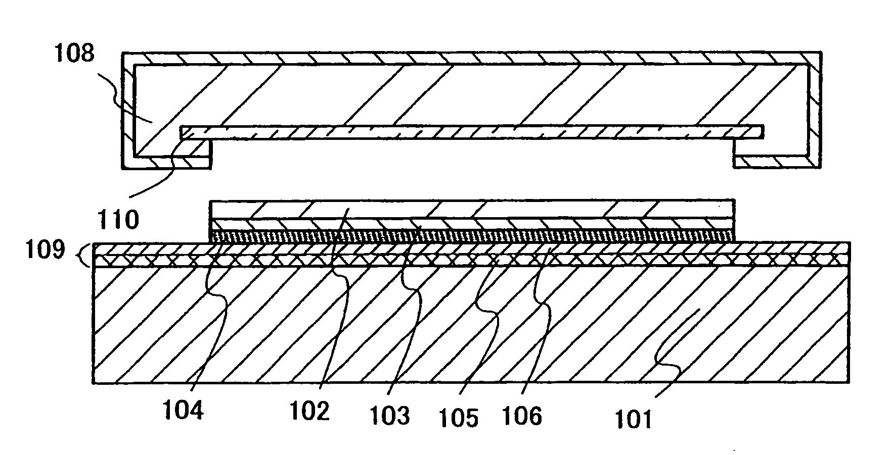
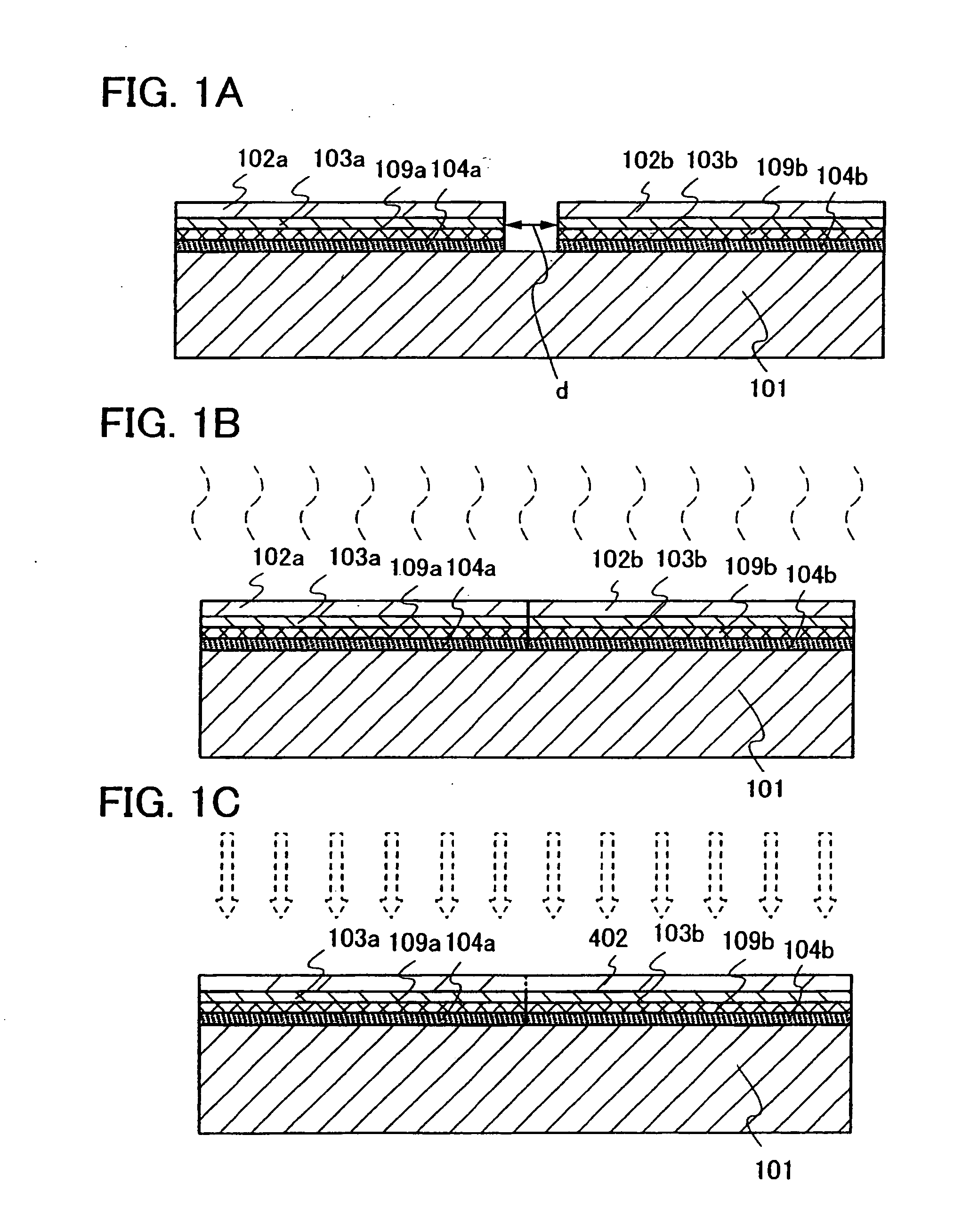
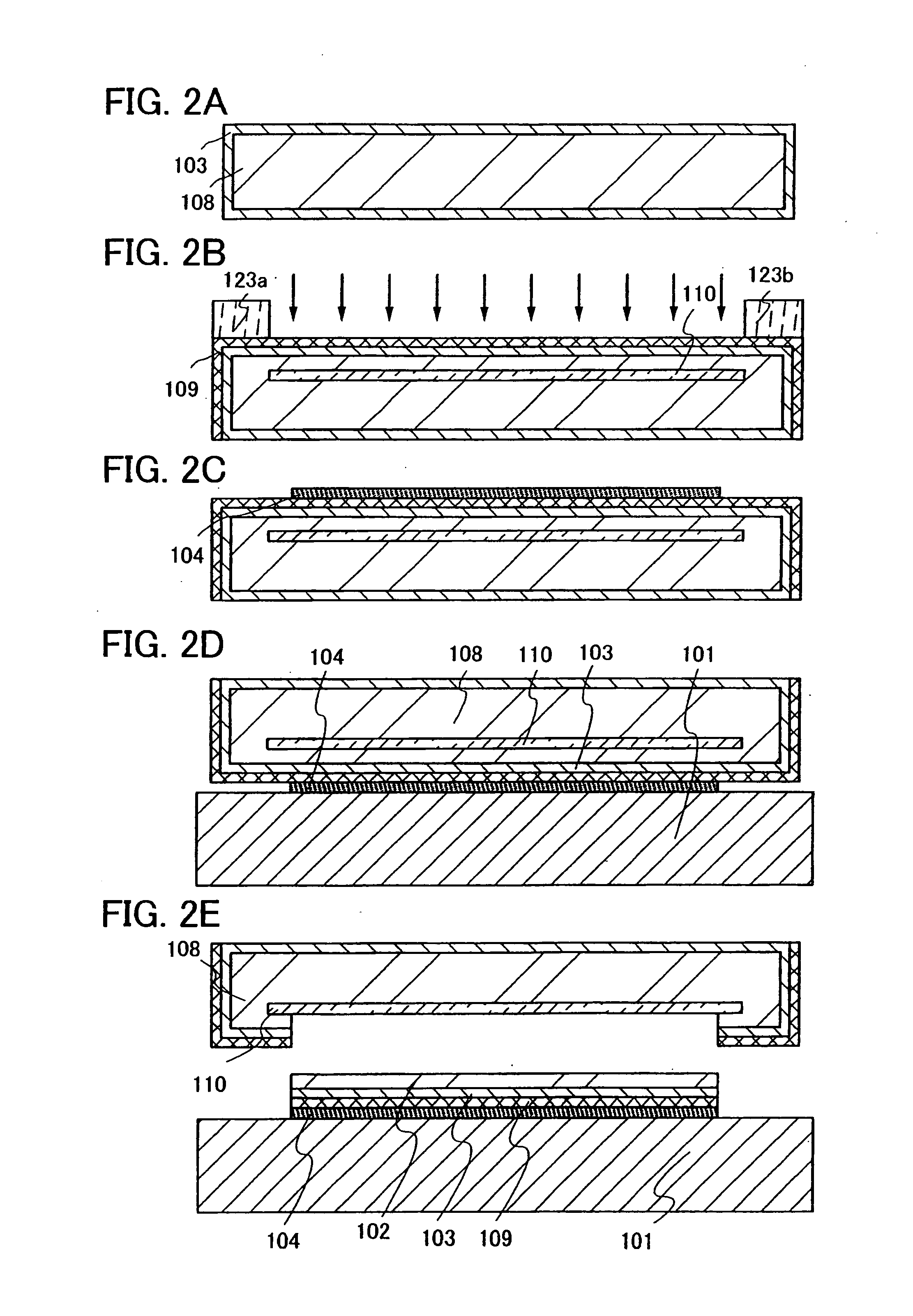
[0061]A method for manufacturing a semiconductor substrate of the present invention will be described with reference to FIGS. 1A to 1C, FIGS. 2A to 2E, and FIGS. 3A to 3D.

[0062]In FIG. 2A, an n-type or p-type single-crystal silicon substrate (a silicon wafer) is typically used as a semiconductor substrate 108. Alternatively, as another crystal semiconductor substrate, a substrate of silicon or germanium, or a substrate of a compound semiconductor such as gallium arsenide or indium phosphide can also be applied. In this embodiment mode, an ion irradiation separation method whereby a crystal semiconductor substrate is irradiated with ions of hydrogen or fluorine to reach a predetermined depth and then heat treatment is performed to separate a single-crystal silicon layer on a surface layer is applied; however, a method whereby epitaxial growth of single-crystal silicon is performed over a porous silicon layer and then the porous silicon layer is separated by water jet may also be appl...

embodiment mode 2

[0144]This embodiment mode will describe an example in which a semiconductor device is manufactured using a single-crystal semiconductor layer which is formed of the single-crystal semiconductor layer where the plurality of single-crystal semiconductor layers formed over the support substrate, which is manufactured in Embodiment Mode 1, are integrated. Specifically, a liquid crystal display device in which a liquid crystal display element is used for a display element will be described. Note that repetitive description of the same portions and portions having the same function as Embodiment Mode 1 will be omitted.

[0145]FIG. 16A is a top view illustrating a structure of a display panel according to the present invention. A pixel portion 2701 in which pixels 2702 are arranged in matrix, a scan line input terminal 2703, and a signal line input terminal 2704 are formed over a substrate 2700 having an insulating surface. The number of pixels may be set in accordance with various standard...

embodiment mode 3

[0204]A semiconductor device having a light-emitting element can be formed by applying the present invention, and the light-emitting element emits light by any one of bottom emission, top emission, and dual emission. This embodiment mode will describe an example of a method for manufacturing a semiconductor device in which a semiconductor device having a display function (also referred to as a display device or a light-emitting device) is manufactured as a bottom-emission, dual-emission, or top-emission semiconductor device having high performance and high reliability with high yield, with reference to FIGS. 8A and 8B, 9, and 10.

[0205]A semiconductor device illustrated in FIGS. 8A and 8B employs a bottom-emission structure in which light is emitted in a direction indicated by an arrow. FIG. 8A is a plan view of the semiconductor device, and FIG. 8B is a cross sectional view taken along line E-F of FIG. 8A. In FIGS. 8A and 8B, the semiconductor device includes an external terminal co...


PUM


Abstract

After the plurality of single-crystal semiconductor layers are provided adjacent to each other with a certain distance over a glass substrate which is a support substrate, heat treatment is performed on the glass substrate. The support substrate shrinks by this heat treatment, and the adjacent single-crystal semiconductor layers are in contact with each other due to the shrink. Energy beam irradiation is performed with the plurality of single-crystal semiconductor layers being in contact with each other, the plurality of single-crystal semiconductor layers are integrated, and thus a continuous single-crystal semiconductor layer is formed.

Description

BACKGROUND OF THE INVENTION[0001]1. Field of the Invention[0002]The present invention relates to a method for manufacturing a silicon-on-insulator (SOI) substrate having a so-called SOI structure in which a semiconductor layer is provided on an insulating surface, and a method for manufacturing semiconductor device having an SOI structure.[0003]2. Description of the Related Art[0004]As an alternative to a silicon wafer which is manufactured by thinly slicing an ingot of a single-crystal semiconductor, an integrated circuit using a semiconductor substrate which is referred to as a silicon on an insulator (hereinafter also referred to as “SOI”) substrate in which a thin single-crystal semiconductor layer is provided on an insulating surface has been developed. The integrated circuit using an SOI substrate has attracted attention as an integrated circuit which reduces parasitic capacitance between a drain of a transistor and the substrate and improves the performance of a semiconductor...

Claims


Application Information

Patent Timeline
IPC IPC(8): H01L21/00
CPCH01L27/1214H01L27/1266
Inventor YAMAZAKI, SHUNPEIARAI, YASUYUKI
Owner SEMICON ENERGY LAB CO LTD
Why Eureka
Try Eureka