Chip assembly
- Summary
- Abstract
- Description
- Claims
- Application Information
AI Technical Summary
Benefits of technology
Problems solved by technology
Method used
Image

Examples
embodiment 1
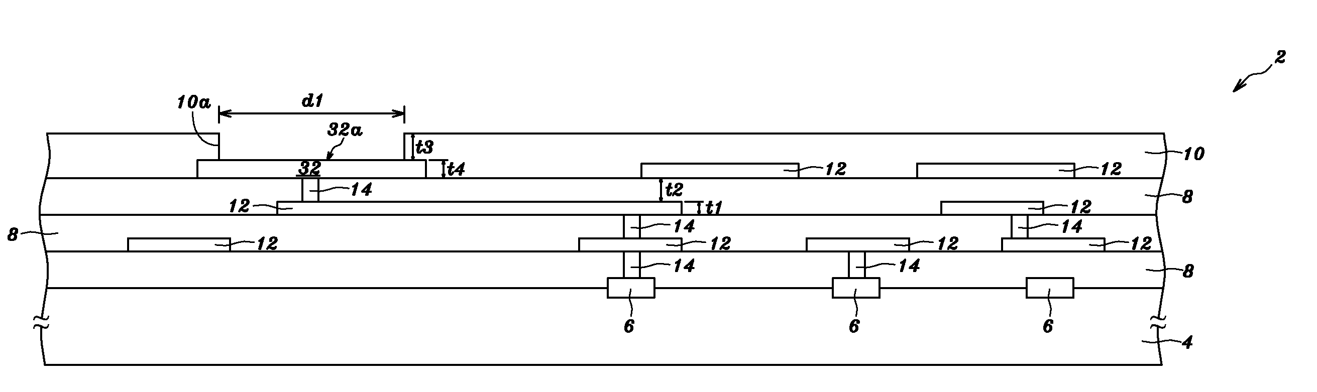
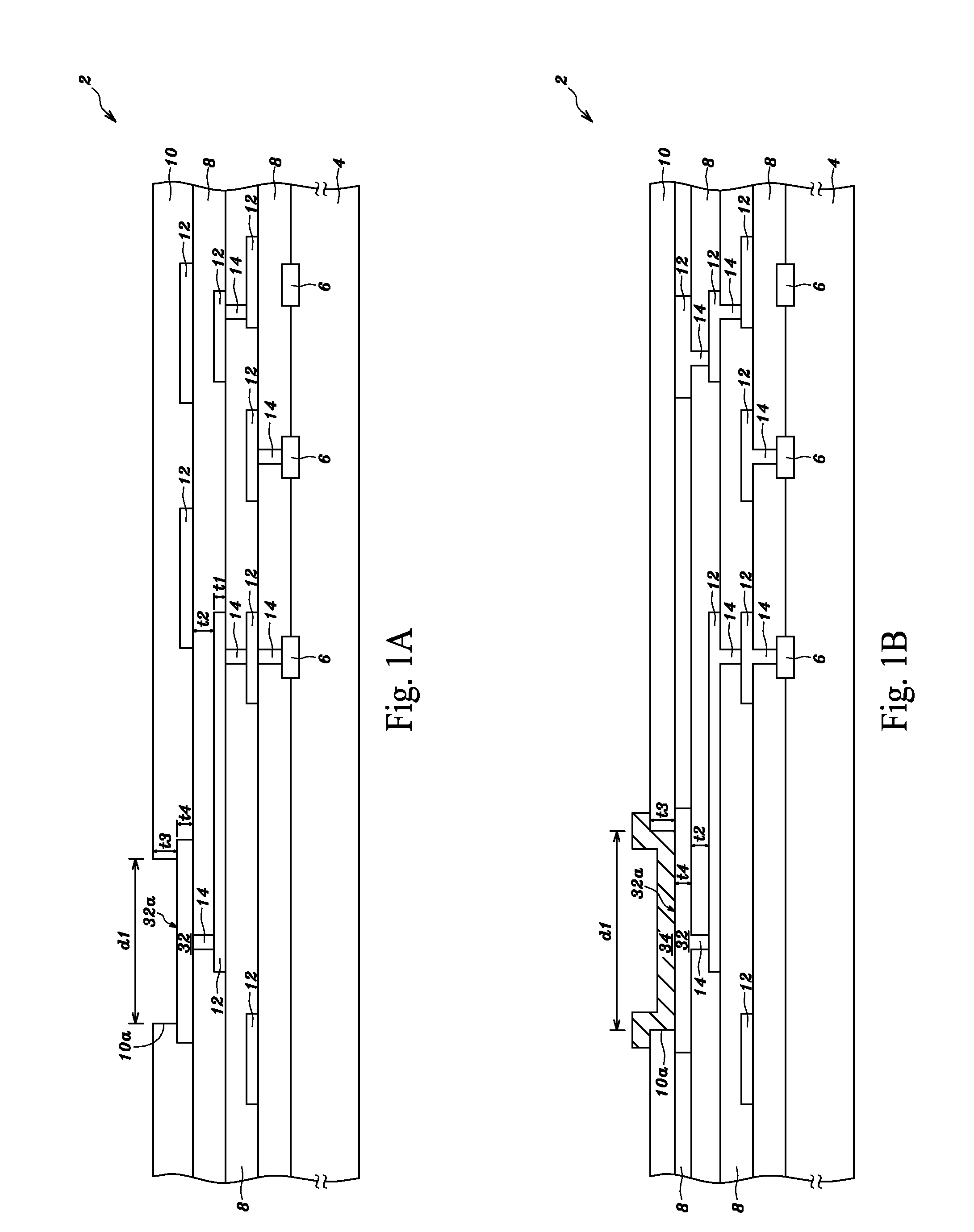
[0075]Referring to FIG. 2A, an adhesion / barrier layer 38 having a thickness of between 0.02 and 0.5 μm, and preferably of between 0.25 and 0.35 μm, can be formed on the passivation layer 10 and on the pads 32, such as aluminum pads or copper pads, exposed by the openings 10a. The adhesion / barrier layer 38 can be formed by a physical vapor deposition (PVD) process, such as a sputtering process or an evaporation process, or a chemical vapor deposition (CVD) process. The material of the adhesion / barrier layer 38 may include titanium, a titanium-tungsten alloy, titanium nitride, chromium, tantalum, tantalum nitride or a composite of the abovementioned materials. In a case, the adhesion / barrier layer 38 can be formed by sputtering a titanium-tungsten-alloy layer with a thickness of between 0.02 and 0.5 μm, and preferably of between 0.25 and 0.35 μm, on the passivation layer 10 and on the pads 32, such as aluminum pads or copper pads, exposed by the openings 10a. In another case, the adhe...
embodiment 2
[0110]Referring to FIG. 3A, the metal bumps 52 can be formed on the metal caps 34, respectively, that is, the adhesion / barrier layer 38 having a thickness of between 0.02 and 0.5 μm, and preferably of between 0.25 and 0.35 μm, can be formed on the passivation layer 10 and on the aluminum-containing layer of the metal caps 34, wherein the aluminum-containing layer may be an aluminum layer, an aluminum-copper-alloy layer or an Al—Si—Cu-alloy layer, followed by forming the seed layer 40, made of copper, having a thickness of between 0.03 and 1 μm, and preferably of between 0.05 and 0.2 μm, on the adhesion / barrier layer 38, followed by the above-mentioned steps as shown in FIGS. 2B-2E. The specification of the adhesion / barrier layer 38 and the seed layer 40 shown in FIG. 3A can be referred to as the specification of the adhesion / barrier layer 38 and the seed layer 40 illustrated in FIG. 2A. The process of forming the adhesion / barrier layer 38, as shown in FIG. 3A, can be referred to as ...
embodiment 3
[0130]Referring to FIG. 4A, multiple metal bumps 114 can be formed on the pads 32, such as copper pads or aluminum pads, exposed by the openings 10a. The process for forming the metal bumps 114 can be performed by the above-mentioned steps as shown in FIGS. 2A-2B, followed by electroplating a copper layer 44 having a thickness of between 5 and 30 micrometers, and preferably of between 10 and 20 micrometers, on the seed layer 40 exposed by the openings 42a, and then electroplating a gold layer 116 having a thickness of between 1 and 10 micrometers, and preferably of between 3 and 6 micrometers, on the electroplated copper layer 44 in the openings 42a with a non-cyanide electroplating solution, such as a solution containing gold sodium sulfite (Na3Au(SO3)2) or a solution containing gold ammonium sulfite ((NH4)3[Au(SO3)2]), or with an electroplating solution containing cyanide, followed by the above-mentioned steps as shown in FIGS. 2D-2E. Thereby, the metal bumps 114 can be formed of ...
PUM
 Abstract
Description
Claims
Application Information
 - R&D
- Intellectual Property
- Life Sciences
- Materials
- Tech Scout
- Unparalleled Data Quality
- Higher Quality Content
- 60% Fewer Hallucinations
Browse by: Latest US Patents, China's latest patents, Technical Efficacy Thesaurus, Application Domain, Technology Topic, Popular Technical Reports.
© 2025 PatSnap. All rights reserved.Legal|Privacy policy|Modern Slavery Act Transparency Statement|Sitemap|About US| Contact US: help@patsnap.com