

Laser Processing Method and Equipment
- Summary
- Abstract
- Description
- Claims
- Application Information
AI Technical Summary
Benefits of technology
Problems solved by technology
Method used
Image

Examples
experiment 1
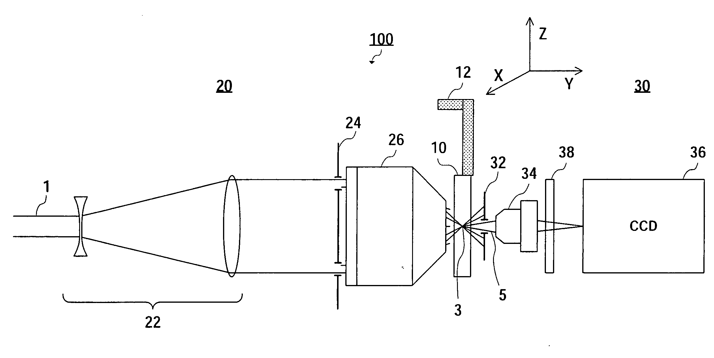
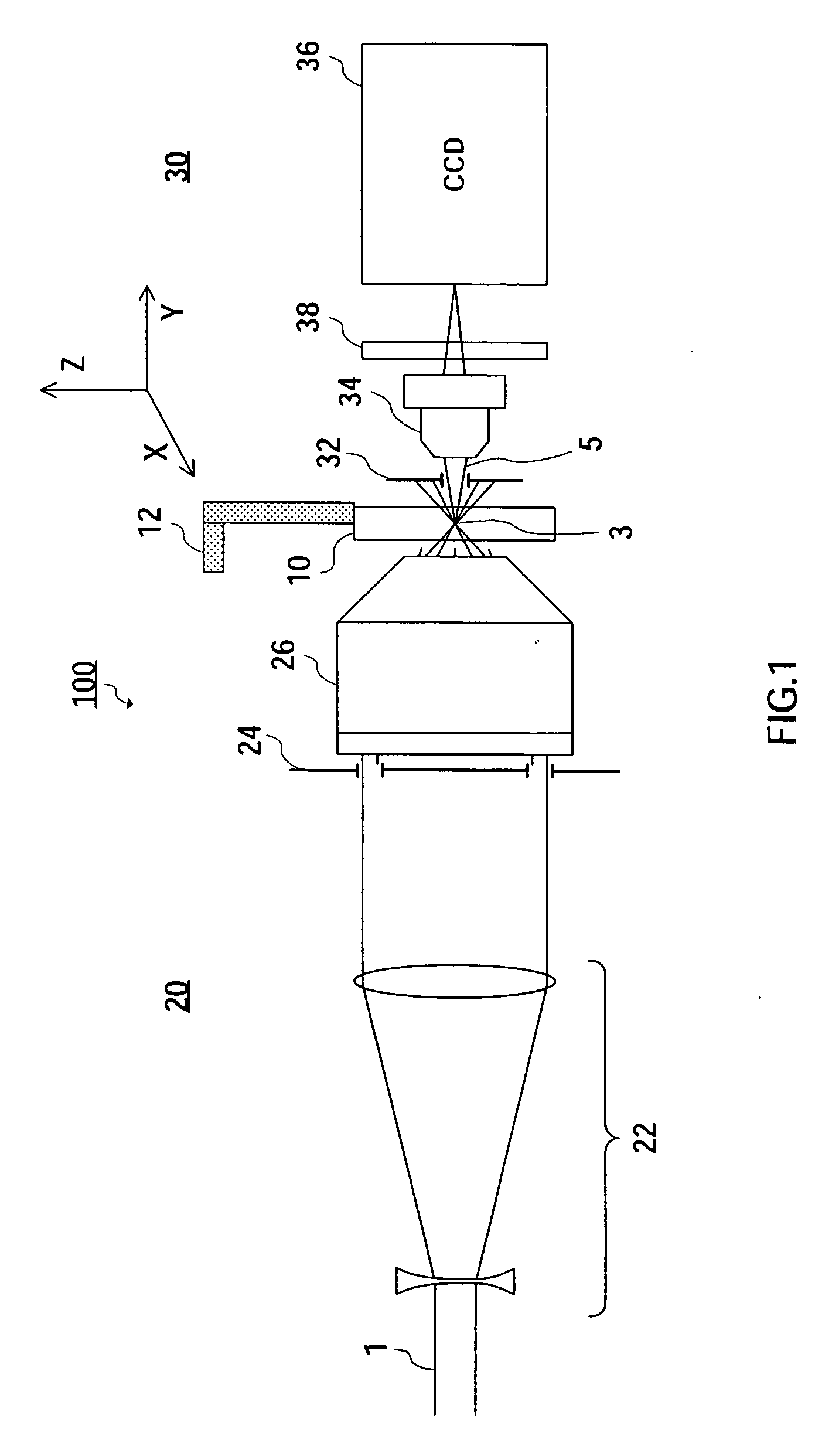
[0053]In Experiment 1, silicate glass (trademark name: BK7) was used as the processing object, and a femtosecond titanium sapphire laser (800 nm wavelength, 150 fs pulse width) was used as the processing laser. It was confirmed that laser beam 1 could be converged to a spot with a diameter of 550 nm, almost equal to the diffraction limit value (800 nm×0.6=480 nm), by the apparatus in FIG. 1. This value was confirmed by a surface convergence control experiment, atomic force microscope (AFM) observation, and numerical simulation.
[0054]Subsequently, damage was all caused by single-shot laser pulse irradiation for one place.
experiment 2
[0055]In Experiment 2, the dependence of glass femtosecond pulse damage on laser intensity was investigated in the same way as in Experiment 1. That is to say, silicate glass (trademark name: BK7) was used as the processing object, and a femtosecond titanium sapphire laser (800 nm wavelength, 150 fs pulse width) was used as the laser. FIG. 4 shows typical examples of dark field scattering images at the laser irradiation location in this case. FIG. 4A shows a light scattering image of damage according to the present invention induced by fluence F of 1.45 J / cm2 (irradiance I of 6.6 TW / cm2), and FIG. 4B shows an image of plasma emission induced by fluence F of 2.1 J / cm2 (irradiance I of 9.4 TW / cm2).
[0056]That is to say, when irradiance I in the irradiated area reached threshold IPth=9.8 TW / cm2, spark-shaped visible light emission was observed in the irradiated area (see FIG. 4B). This is plasma occurrence due to laser convergence of the kind also observed in the technology described in...
experiment 3
[0058]In Experiment 3, the dependence of the threshold of damage laser intensity (irradiance) according to the present invention on the pulse width was investigated for glass (BK7 glass, for example). The pulsed lasers used were a femtosecond titanium sapphire laser (800 nm wavelength, 150 fs pulse width), a picosecond Nd:YAG laser (1064 nm wavelength, 30 ps pulse width), a nanosecond Nd:YAG laser (1064 nm wavelength, 10 ns pulse width), and so forth. As a result, it was found that damage irradiance threshold Idth maintained an almost fixed value of 6 TW / cm2 over a wide range of pulse widths from 100 femtoseconds to 30 nanoseconds, as shown in FIG. 5A. That is to say, it was found that damage irradiance threshold Idth is not at all dependent on pulse width τ of the pulsed laser used, but has an almost fixed value. This is an important experimental fact that characterizes damage according to the present invention.
[0059]For comparison, in FIG. 5B the dependence of the fluence threshol...
PUM
| Property | Measurement | Unit |
|---|---|---|
| Time | aaaaa | aaaaa |
| Time | aaaaa | aaaaa |
| Diameter | aaaaa | aaaaa |
Abstract
Description
Claims
Application Information