Photodiode, solid state image sensor, and method of manufacturing the same
- Summary
- Abstract
- Description
- Claims
- Application Information
AI Technical Summary
Benefits of technology
Problems solved by technology
Method used
Image
Examples
first embodiment
[0064]FIGS. 6A through 6C are plan views showing a configuration of a solid state image sensing device 20 according to a first embodiment of the present invention. FIGS. 7A through 7D are cross-sectional views taken along the lines A-A′, B-B′, C-C′, and D-D′, respectively, in FIGS. 6A through 6C. Of those, FIG. 6A shows a plan view showing an overall configuration of the solid state image sensing device 20, and FIGS. 6B and 6C show plan views of an n-channel MOS transistor and a p-channel MOS transistor, respectively, which are not shown in the plan view of FIG. 6A and form a CMOS logic element that cooperates with the solid state image sensing device 20.
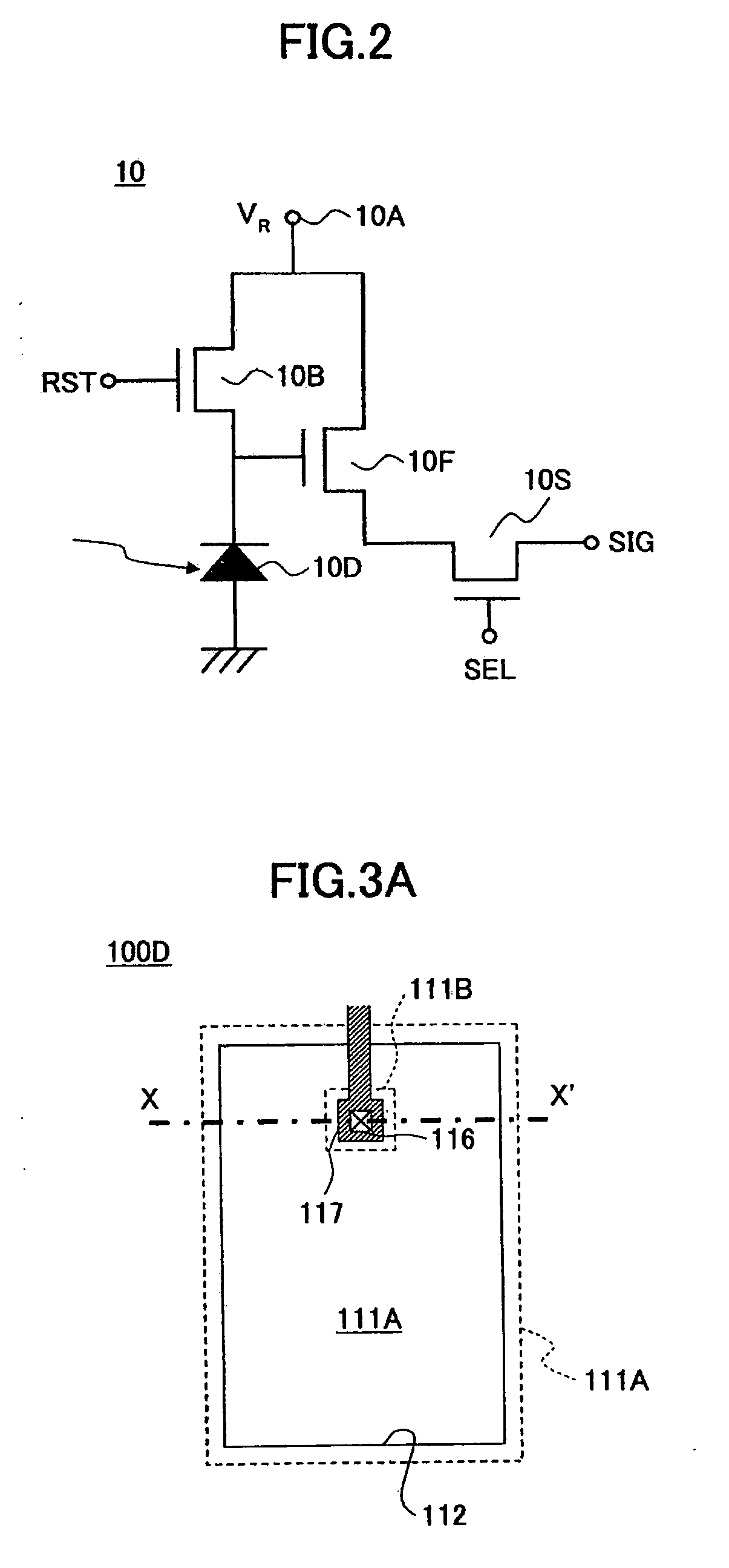
[0065]Referring to FIG. 6A and FIG. 7A, the solid state image sensing device 20 corresponds to the equivalent circuit diagram of the light-receiving element shown above in FIG. 2, and has the photodiode 10D and the reset transistor 10B connected in series to an interconnect pattern forming the power supply terminal 10A. Further, the...
second embodiment
[0086]Next, referring to FIGS. 8A through 8U, a description is given, with respect to each of the device regions 30, 40, 60, and 80, of a manufacturing process of the solid state image sensing device of FIGS. 6A through 6C as a second embodiment of the present invention.
[0087]In the process of FIG. 8A, the isolation oxide film 22 of 300 nm in thickness is formed on the p-type silicon substrate 21 by LOCOS so that the device regions 30, 40, 60, and 80 are defined. For example, a silicon epitaxial layer having a resistivity of 10 to 100 Ωcm and a thickness of 5 to 12 μm may be formed and used as the p-type silicon substrate 21.
[0088]Next, in the process of FIG. 8B, a resist pattern R1 that exposes only the device region 60 is formed on the structure of FIG. 8A, and the p-type well 61A is formed in the device region 60 by performing ion implantation of B+ ions, using the resist pattern R1 as a mask, first at a dose of 1×10¹³ to 5×1013 cm−2 at an acceleration voltage of 250 to 600 keV, ...
PUM
 Abstract
Description
Claims
Application Information


