

Pattern forming method
- Summary
- Abstract
- Description
- Claims
- Application Information
AI Technical Summary
Benefits of technology
Problems solved by technology
Method used
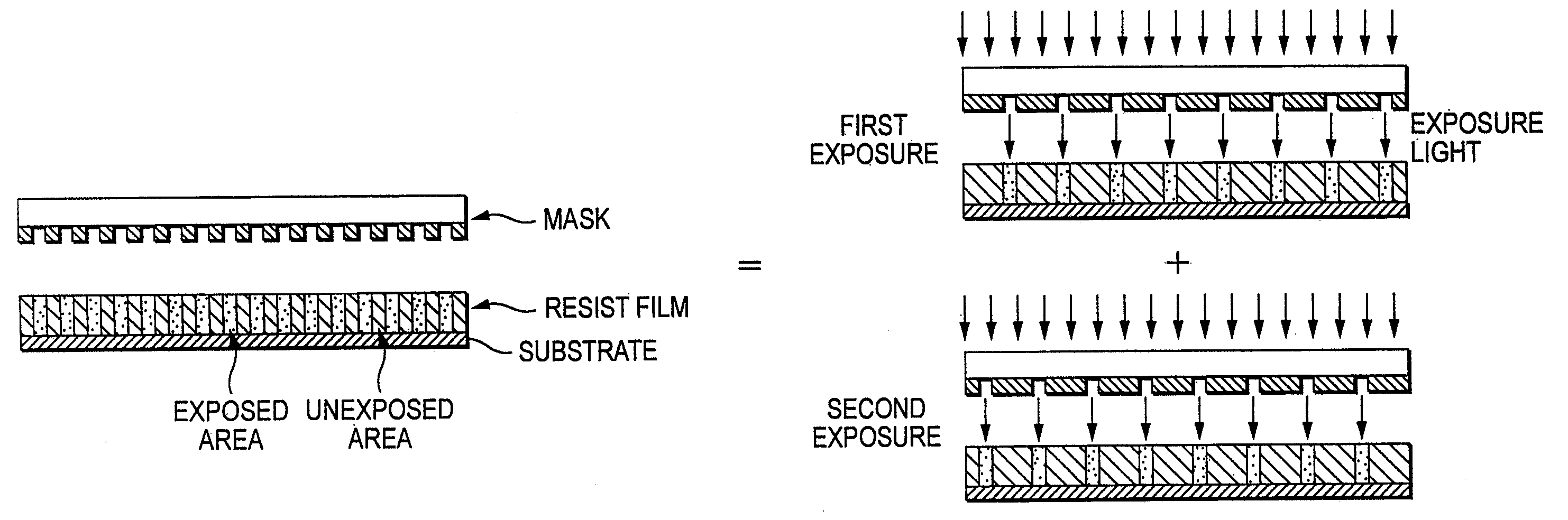
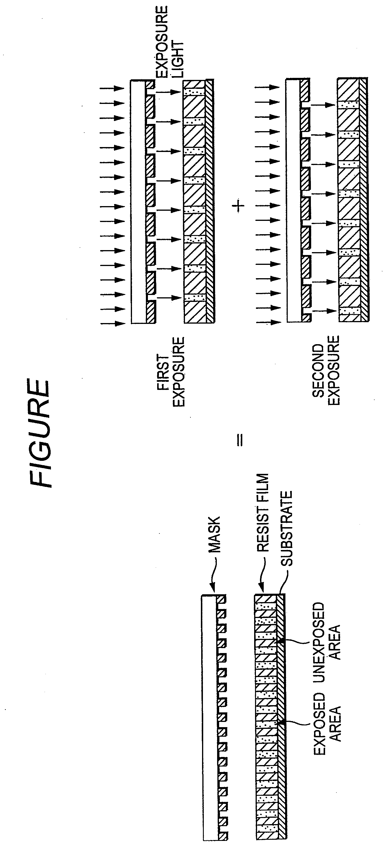
Image

Examples
synthesis example 1
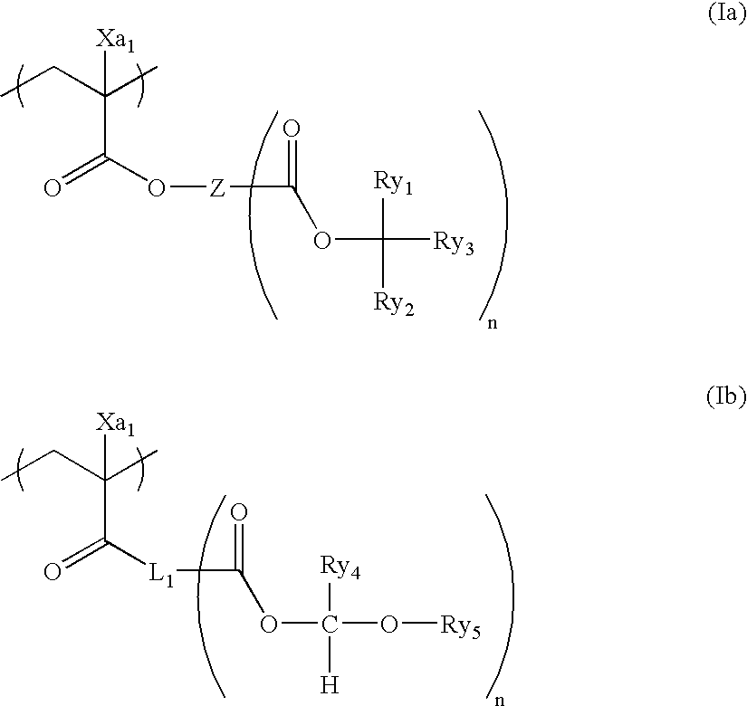
Synthesis of Resin (1)
[0461]Under a nitrogen stream, 8.8 g of cyclohexanone was charged into a three-neck flask and heated at 80° C. Thereto, a solution prepared by dissolving 8.5 g of γ-butyrolactone methacrylate, 4.7 g of 3-hydroxyadamantyl-1-methacrylate, 8.8 g of 2-methyl-2-adamantyloxycarbonylmethyl methacrylate, and polymerization initiator V-60 (produced by Wako Pure Chemical Industries, Ltd.) in an amount of 13 mol % based on the monomer, in 79 g of cyclohexanone was added dropwise over 6 hours. After the completion of dropwise addition, the reaction was further allowed to proceed at 80° C. for 2 hours. The reaction solution was left standing to cool and then added dropwise to a mixed solution of 900-ml methanol / 100-ml water over 20 minutes, and the precipitated powder material was collected by filtration and dried to obtain 18 g of Resin (1). The weight average molecular weight of Resin (1) obtained was 6,200 in terms of standard polystyrene, and the dispersity (Mw / Mn) was ...
PUM
 Abstract
Description
Claims
Application Information