
Sensing Device, Sensing Apparatus, and Sensing Method

a sensing device and sensing technology, applied in the direction of luminescent dosimeters, optical radiation measurement, fluorescence/phosphorescence, etc., can solve the problem of difficult to achieve multiphoton excitation efficiency, difficult to actually improve the excitation rate of multiphoton excitation, and the approach to implement multiphoton excitation and plasmon enhancing effect with high efficiency is limited in its effect to a certain level, so as to enhance optical response, enhance optical response, and enhance sensitivity

Inactive Publication Date: 2009-02-05
HOKKAIDO UNIVERSITY
View PDF3 Cites 14 Cited by
  • Summary
  • Abstract
  • Description
  • Claims
  • Application Information

AI Technical Summary

Problems solved by technology

Accordingly, even with the localized plasmon enhancement effect, it is difficult to efficiently induce multiphoton excitation.
Further, although combining multiphoton absorption and the localized plasmon enhancing effect is an excellent idea for highly sensitive optical detection, it is very difficult to actually improve the excitation rate in multiphoton excitation as described above.
In other words, the approach that has been performed to implement multiphoton excitation and plasmon enhancing effect with high efficiency is limited in its effect to a certain level.
This is based on the fact that the knowledge virtually lacks about optimal structures of a metal structure (specifically, fine metal particles exhibiting plasmon resonance absorption arranged on the metal structure) that is an element of sensing-target systems.
For example, if it is possible to provide spectral sensitivity functions to an optical response sensor, great improvements in the sensitivity of sensing can be expected by selecting a wavelength of an excitation light source to use, but providing such functions has actually been difficult.
Further, high sensitivity sensing has generally been difficult.

Method used


Image

  • Sensing Device, Sensing Apparatus, and Sensing Method
  • Sensing Device, Sensing Apparatus, and Sensing Method
  • Sensing Device, Sensing Apparatus, and Sensing Method

Examples


example 1

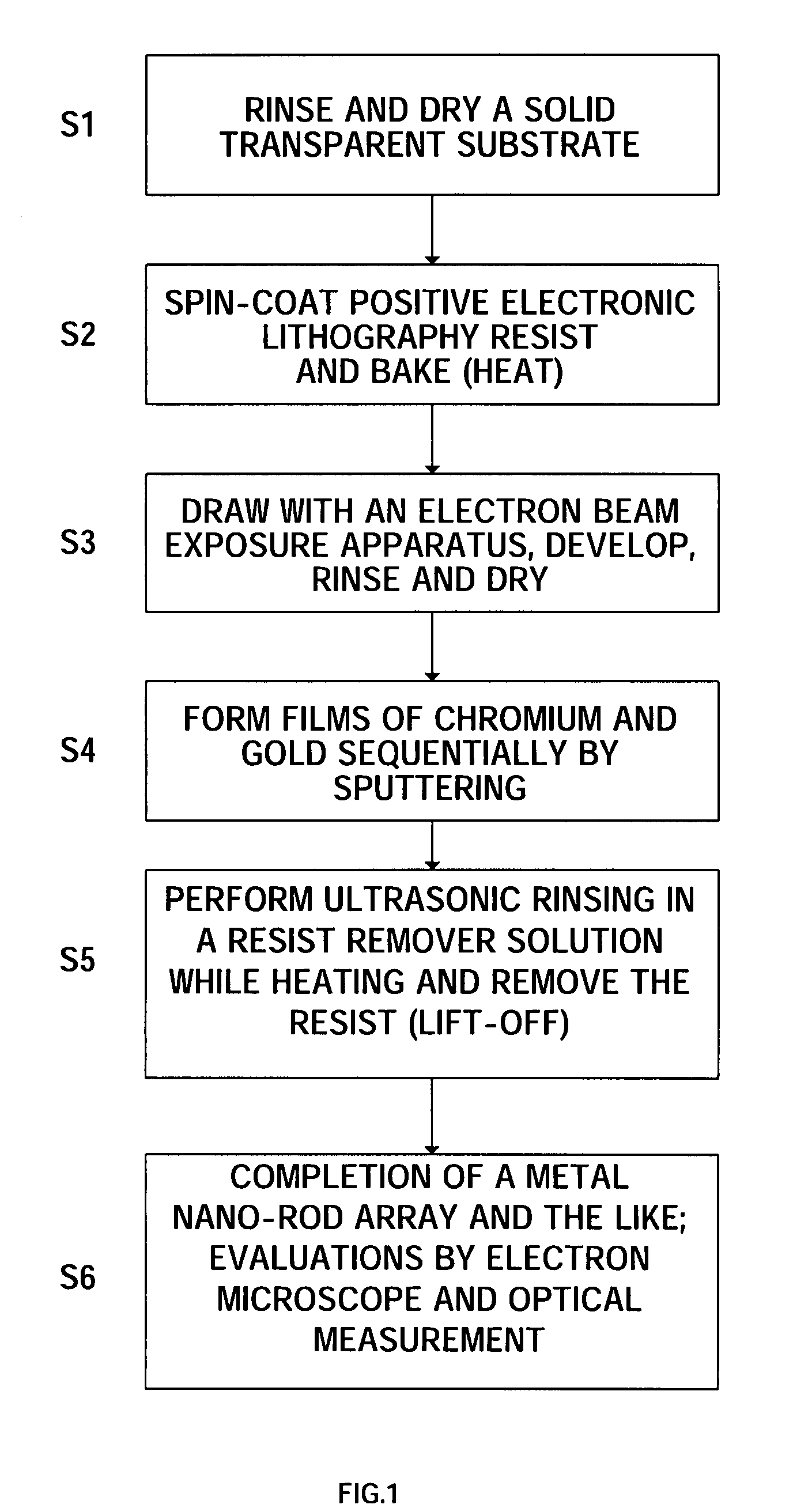
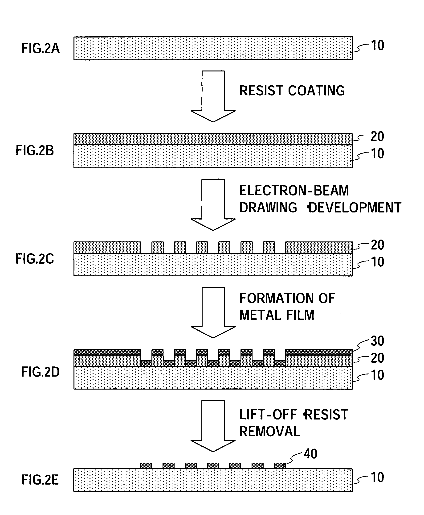
[0136]In this example, fine metal particles were fabricated on a glass substrate (Matsunami Glass: 24 mm×24 mm) by electron-beam lithography / lift-off. More specifically, the glass substrate was subjected to ultrasonic rinsing with acetone, methanol, and pure water in this order, and a positive electron-beam lithography resist (ZEP-520A, Zeon corporation, diluted to two parts of a dedicated thinner) was spin-coated (initial: 1000 rpm for 10 sec. main: 4000 rpm for 90 sec.) on the glass substrate, and was pre-baked at 180° C. for 3 minutes on a hot plate. Next, a predetermined pattern was drawn at a dose rate of 1.2 μC / cm2 using an electron beam exposure apparatus with the acceleration voltage of 100 kV, and developed for 30 minutes. Next, 2 nm of chromium and 10 nm to 100 nm of gold were deposited on the developed and rinsed substrate by sputtering, and lift-off was performed in a resist remover solution (dimethylformamide). At this point, by applying ultrasonic waves for 5 minutes w...

example 2

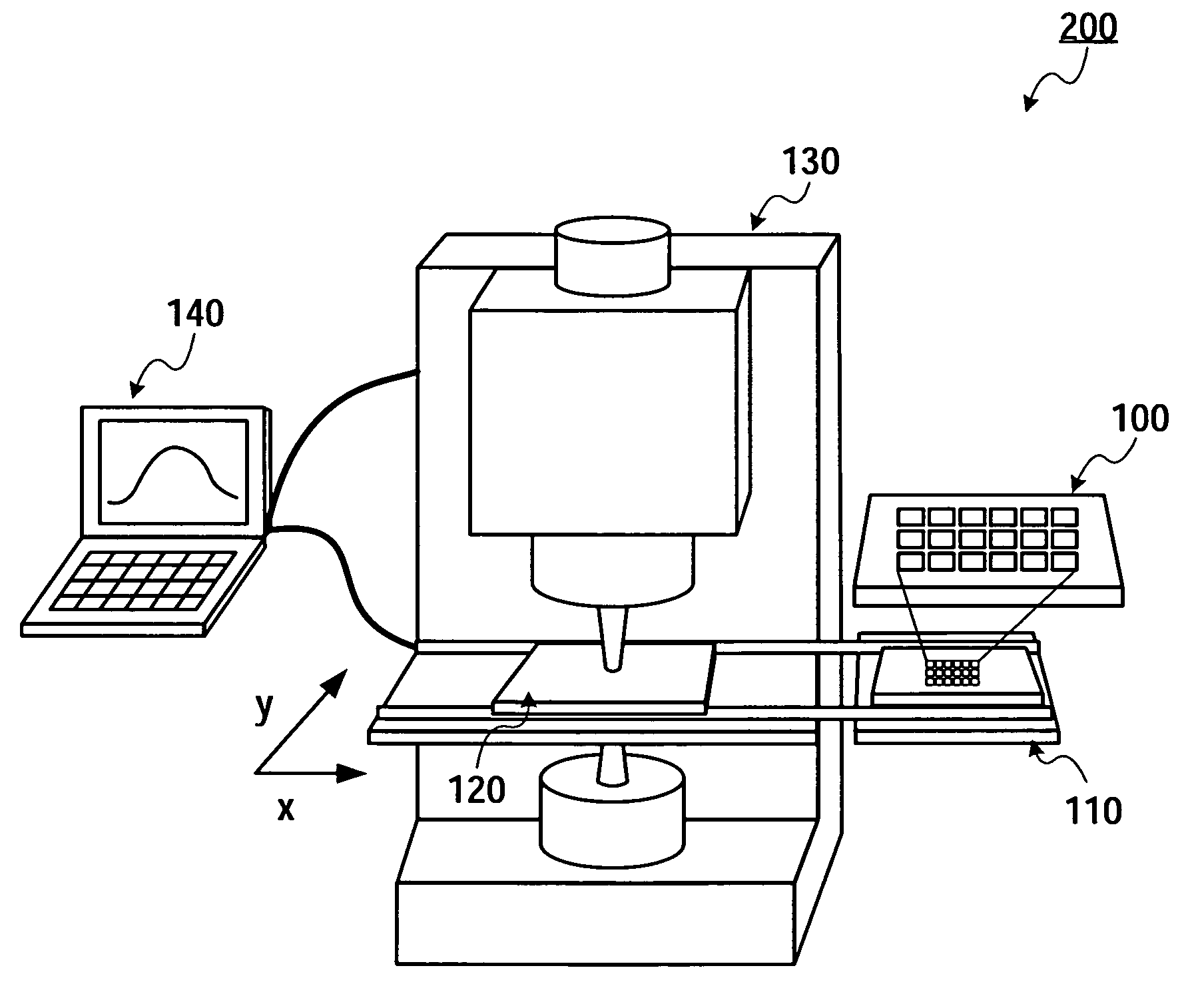
[0145]The present inventors further performed experiments on multiphoton excitation efficiency and fluorescence enhancement of the metal structures (sensing devices) fabricated by the method.

[0146]The present inventors have fabricated a metal structure such that the thickness, the length of the long axis and the length of the short axis of each fine metal particle was constant and that the distance between adjoining fine metal particles was only varied, and examined multiphoton excitation efficiency and fluorescence enhancement of these metal structures.

[0147]FIG. 11 is an electron microscope photograph of a metal structure where fine metal particles with various gaps are formed integrally. Figures (0 nm, 2 nm, 4 nm, 6 nm, 8 nm, 10 nm, 20 nm, 30 nm and 40 nm) shown in FIG. 11 are distances between respective adjoining fine metal particles. The long axis and short axis of each of the fine metal particles were 100 nm, and the thickness thereof was 40 nm.

[0148]After making dye (1,4-Bis...

example 3

[0159]In this Example, fine metal particles were fabricated on a glass substrate with the design of the long axis and short axis of both 80 nm and the distance between fine metal particles of 4 nm. First, DNA (1 mmol / l) with thiol modified at 3′ end of 40 base pairs was dropped onto the glass substrate, and the glass substrate was allowed to stand in an incubator of 37° C. for 12 hours to induce coupling to gold. Next, complementary DNA was allowed to stand in a buffer of pH7.4 at 37° C. to induce hybridization. Then, the metal structure was slowly stirred three times each for 5 minutes in a surfactant solution (sodium dodecyl sulphate, SDS solution) and rinsed, SYBR Green (Molecular Probes, Inc.) was diluted to 1000 parts of dimethyl sulfoxide (DMSO) and dropped onto the metal structure, and the metal structure was rinsed by the surfactant solution in the same way as described above ten minutes later. The measurement system was the same as described above.

[0160]Then, the fabricated...


PUM

PropertyMeasurementUnit
distanceaaaaaaaaaa
heightaaaaaaaaaa
heightaaaaaaaaaa

Abstract

There are provided a sensing device, a sensing apparatus, and a sensing method capable of realizing effective multi-photon absorption and local plasmon enhancement function. The sensing device can realize a high multi-photon excitation efficiency and selectivity by accurately controlling the material, shape, size, interval, and direction of metal particles arranged on a substrate. By employing the sensing device in various sensing apparatuses such as a fluorescent sensing apparatus, it is possible to realize sensing of detection object material with a high sensibility.

Description

TECHNICAL FIELD[0001]The present invention relates to a sensing device, sensing apparatus and sensing method. More particularly, the present invention relates to a sensing device, sensing apparatus and sensing method for enhancing optical response from various kinds of sensing-target objects by surface (localized) plasmon and performing highly sensitive optical detection.BACKGROUND ART[0002]Fine metals (including, for example, fine metals having surface structures of the scale of nanometers and fine metal particles of the size of nanometers) exhibit a characteristic optical response. (optical absorption), called “localized (surface) plasmon resonance absorption,” in a specific wavelength range, according to their shape and size. Examples of metals exhibiting localized plasmon resonance absorption include precious metals such as gold, silver and platinum, and it is important that the plasmon resonance absorption wavelength changes according to the size and shape even for the same kin...

Claims


Application Information

Patent Timeline
Patent Type & Authority Applications(United States)
IPC IPC(8): G01N21/64
CPCG01N21/648G01N21/6428Y10S977/773Y10S977/774Y10S977/778Y10S977/779
Inventor MISAWA, HIROAKIUENO, KOSEITSUBOI, YASUYUKISASAKI, KEIJI
Owner HOKKAIDO UNIVERSITY
Learn More