
Electron transporting materials and organic light-emitting devices therewith

a technology electron transporting materials, which is applied in the direction of discharge tubes/lamp details, organic chemistry, discharge tubes luminescnet screens, etc., can solve the problems of low heat resistance of organic light-emitting devices, high crystallinity, and difficulty in retaining an amorphous thin film, so as to achieve stable thin films and reduce voltage. , the effect of high heat resistan

Inactive Publication Date: 2009-02-12
YAMAGATA PROMOTIONAL ORG FOR INDAL TECH
View PDF3 Cites 2 Cited by
  • Summary
  • Abstract
  • Description
  • Claims
  • Application Information

AI Technical Summary

Benefits of technology

"The present invention provides novel electron transporting materials with high thermal characteristics for use in organic light-emitting devices. These materials have high heat resistance and can form stable thin films with low voltage and increased device efficiency. The invention also provides organic light-emitting devices with high reliability, particularly for applications requiring long-term, stable lighting such as flat panel displays and lighting fixtures."

Problems solved by technology

However, the conventional materials described in each patent or non-patent document have problems such as a planar structure, high crystallinity and difficulty in retaining an amorphous thin film.
Such low heat resistance of components of organic light-emitting devices is a significant problem with facsimiles, copying machines, backlights for liquid crystal displays, and light sources such as lights and also undesirable for display devices such as full-color flat-panel displays.

Method used


Image

  • Electron transporting materials and organic light-emitting devices therewith
  • Electron transporting materials and organic light-emitting devices therewith
  • Electron transporting materials and organic light-emitting devices therewith

Examples


example 1

Synthesis of DPF

[0106]DPF was synthesized according to the synthesis scheme shown below under the title of Chemical Formula 20.

[0107]First, 12.5 g (75.39 mmol) of fluorene, 21.0 g (173.4 mmol) of 4-cyanofluorobenzene, DMF, and 1.0 g (7.52 mmol) of potassium carbonate were added in this order to a flask and allowed to react under a nitrogen atmosphere at 125° C. for 22 hours.

[0108]The reaction solution was filtrated, and the resulting filtrate was subjected to reprecipitation with methanol. The precipitated crystal was separated by filtration, washed with methanol and dried in a dryer.

[0109]As a result of mass spectrometry (MS) and 1H-NMR analysis, the resulting crystal was identified as the target product, 9,9′-bis(4-cyanophenyl)fluorene. The amount of the product was 12.2 g, and the yield was 43.9% based on the amount of fluorene.

[0110]Thereafter, 5.5 g (14.93 mmol) of the resulting 9,9′-bis(4-cyanophenyl)fluorene and TFT were added to a reaction vessel and stirred under a nitrogen...

example 2

Synthesis of DPF

[0140]DPF was synthesized according to the synthesis scheme shown below under the title of Chemical Formula 21.

[0141]First, 5.0 g (30.08 mmol) of fluorene, 8.4 g (69.18 mmol) of 3-cyanofluorobenzene, 24.5 g (75.2 mmol) of cesium carbonate, and DMF were added in this order to a reaction vessel and allowed to react under a nitrogen atmosphere at 150° C. for 22 hours.

[0142]The reaction solution was filtrated, and DMF was removed. The residue was then purified on a silica gel column developed with a mixed solvent of ethyl acetate / n-hexane.

[0143]As a result of MS and 1H-NMR analysis, the purified product in the form of yellow sticky powder was identified as the target product, 9,9′-bis(3-cyanophenyl)fluorene. The amount of the product was 5.1 g (46.5% yield).

[0144]To a flask was added 70 ml of a 1 mol / l THF solution of methyl magnesium bromide, and the air was replaced by a nitrogen atmosphere. A solution of 5.1 g (14.01 mmol) of the resulting 9,9′-bis(3-cyanophenyl)fluor...

example 3

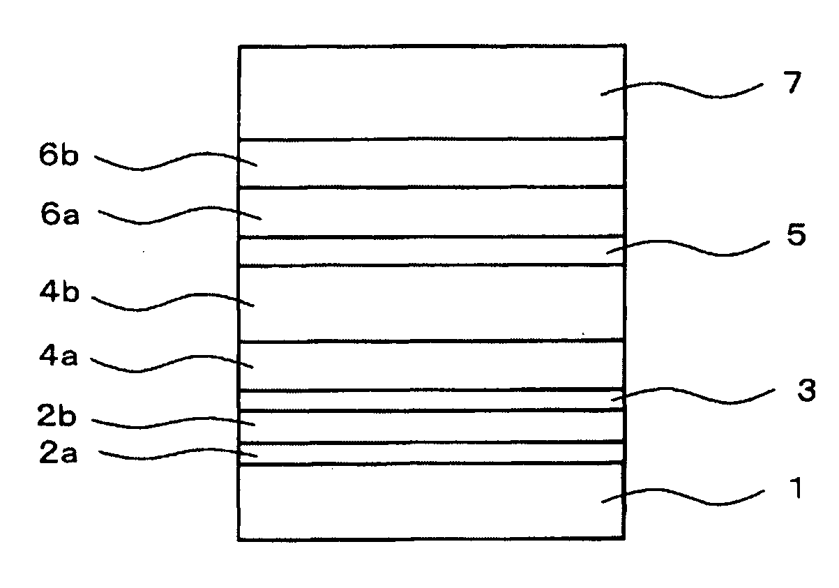
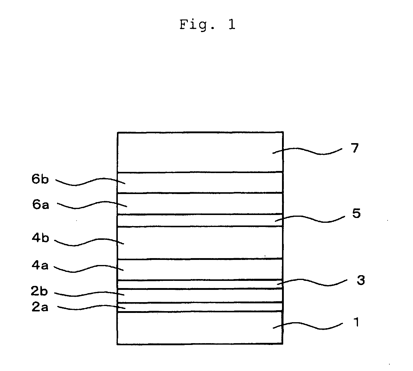
[0159]An organic light-emitting device having the layered structure shown in FIG. 1 was prepared using the process of Example 1, except that the m-DPF synthesized in Example 2 was used as the electron transporting material.

[0160]Briefly, the layered structure of the device is as follows: ITO (110 nm) / NS21:MoO3 (10 nm, 80:20) / NS21:MoO3 (20 nm, 90:10) / NS21 (5 nm) / NS21:EY52 (20 nm, 98.7:1.3) / EB43:EB52 (30 nm, 98.8:1.2) / m-DPF (20 nm) / m-DPF:Liq (10 nm, 74:26) / Al (100 nm).


PUM

PropertyMeasurementUnit
Tgaaaaaaaaaa
melting pointsaaaaaaaaaa

Abstract

The present invention provides a novel electron transporting material having good heat resistance and being capable of forming devices with high thermal characteristics and an organic light-emitting device therewith. The phenanthroline derivative represented by the general formula below is used as the electron transporting material to form the organic light-emitting device:wherein the position of the substituent R6 or R7 depends on the position of the linkage between the phenanthrolinyl group and the fluorenyl group; X represents a single bond between the phenanthrolinyl group and the fluorenyl group; n0 and n1 each independently represent an integer of 0 to 2; and n2 and n3 each represent the number of the substituents and each independently represent an integer of 1 to 4.

Description

BACKGROUND OF THE INVENTION[0001]1. Field of the Invention[0002]The present invention relates to novel electron transporting materials including phenanthroline derivatives and to organic light-emitting devices therewith.[0003]2. Description of the Related Art[0004]Organic light-emitting devices, which are self-luminescence devices using organic compounds as luminescent materials, are characterized in that they are suitable for movie display because of their ability to emit light at high speed and that they can form thin display panels because of their simple structure. Organic light-emitting devices having such good characteristics are becoming widespread in daily-life applications such as cellular phones and car displays.[0005]Organic light-emitting devices have a basic layered structure of anode / light-emitting layer / cathode, in which a layer containing a hole or electron transporting material having the function of transporting holes or electrons is generally placed in order to in...

Claims


Application Information

Patent Timeline
Patent Type & Authority Applications(United States)
IPC IPC(8): H01J1/63C07D471/02H01J1/62
CPCC07D471/04C07D519/00H05B33/14H01L51/0072H01L51/5048C09K11/06H10K85/6572H10K50/14
Inventor KIMURA, MASATOODA, ATSUSHIKIDO, JUNJI
Owner YAMAGATA PROMOTIONAL ORG FOR INDAL TECH
Learn More