Composition for forming passivation layer and organic thin film transistor comprising the passivation layer

a technology of organic thin film transistor and passivation layer, which is applied in the direction of polyether coating, printing, gas-filled discharge tubes, etc., can solve the problems of difficult forming patterns through a solution process, no effective method of forming passivation layers on organic thin film transistors, and deterioration of semiconductors, so as to prevent or reduce the degradation of organic thin films, prevent or reduce the infiltration of oxygen and moisture, and form patterns more easily

Inactive Publication Date: 2009-02-19
SAMSUNG ELECTRONICS CO LTD
View PDF3 Cites 13 Cited by
  • Summary
  • Abstract
  • Description
  • Claims
  • Application Information

AI Technical Summary

Benefits of technology

[0009]Accordingly, example embodiments have been made keeping in mind the above problems occurring in the prior art, and example embodiments provide a composition which prevents or reduces the infiltration of oxygen and moisture, and thus may constantly maintain the initial performance of an organic thin film transistor, prevent or reduce the degradation of an organic thin film, and be formed into patterns more easily.

Problems solved by technology

Currently, there may be no effective method of forming a passivation layer on an organic thin film transistor.
This method may be advantageous in that the film quality may be improved, but may be problematic in that the interfacial characteristics of the organic semiconductor may be deteriorated, forming a pattern through a solution process may be difficult, and performing a vacuum process and a high-temperature process may be difficult.
In particular, this method may be problematic in that an organic semiconductor active layer may be deteriorated by active gas or plasma, and thus the performance of the organic thin film transistor may rapidly worsen.
However, in this method, because the heat-treatment temperature may be about 150° C. or more, an organic active layer may be rapidly deteriorated at increased temperatures, and thus this method may not be an effective method for forming a passivation layer of an organic thin film transistor.
In particular, the most important problem in the method of forming a passivation layer of an organic thin film transistor using an organic film may be that the materials for forming the passivation layer may directly come into contact with an organic active layer, and thus the deterioration of an organic semiconductor active layer may be accelerated by an organic solvent.
Further, in this method, the charge mobility after processing may be rapidly decreased to about ⅓. Accordingly, when a passivation layer is formed using an organic film or an inorganic film through the above methods, there may be a limit in that the initial performance of an organic thin film transistor may be maintained.

Method used


Image

  • Composition for forming passivation layer and organic thin film transistor comprising the passivation layer
  • Composition for forming passivation layer and organic thin film transistor comprising the passivation layer
  • Composition for forming passivation layer and organic thin film transistor comprising the passivation layer

Examples


example 1

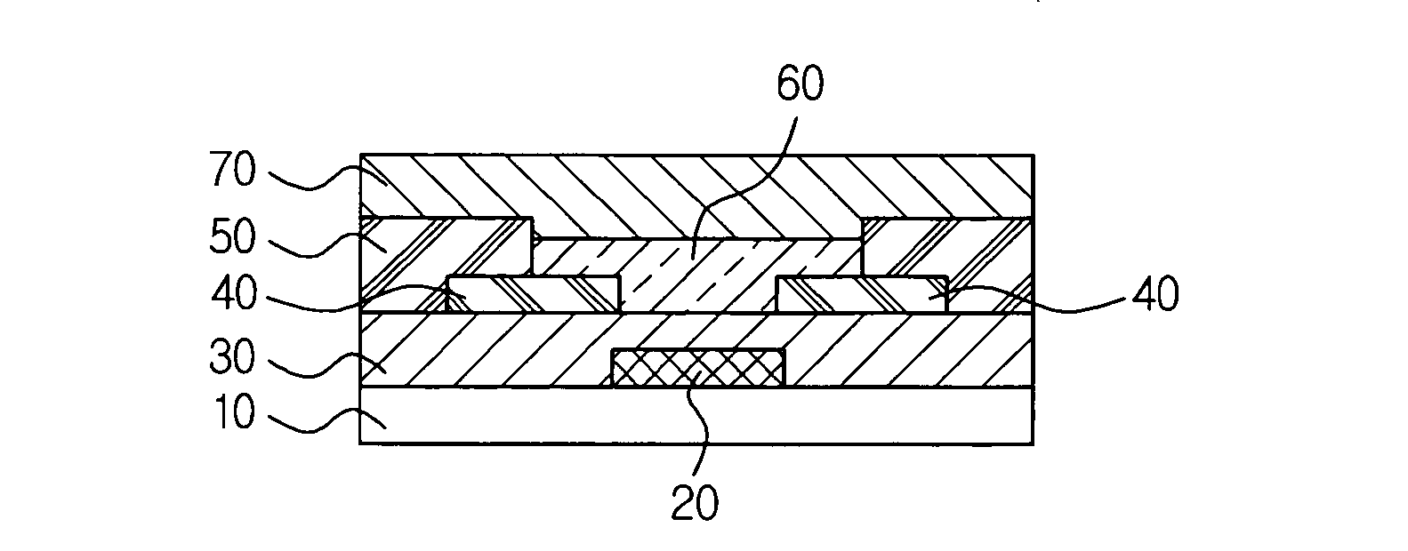
[0057]First, a gate electrode having a thickness of about 1500 Å was formed on a cleaned glass substrate using aluminum (Al) through a sputtering method. Then, polyvinyl phenol was applied on the gate electrode to a thickness of about 4000 Å at a rotation speed of about 2000 rpm using a spin coating method, and was then baked at a temperature of about 70° C. for about 15 minutes, and at a temperature of about 180° C. for about 2 hours, thus forming an organic gate insulation film. Thereafter, gold (Au) was deposited on the organic gate insulation film to a thickness of about 700 Å under conditions of a vacuum of about 2×10⁻⁷ torr and a deposition rate of about 5 Å / sec using a thermal evaporation method, and then an Au electrode pattern was formed through a photolithography process.

[0058]Subsequently, a bank was formed by applying photoacryl on the Au electrode using a spin-coating method. Thereafter, an organic semiconductor active layer was formed by layering polythiophene, which m...

experimental example

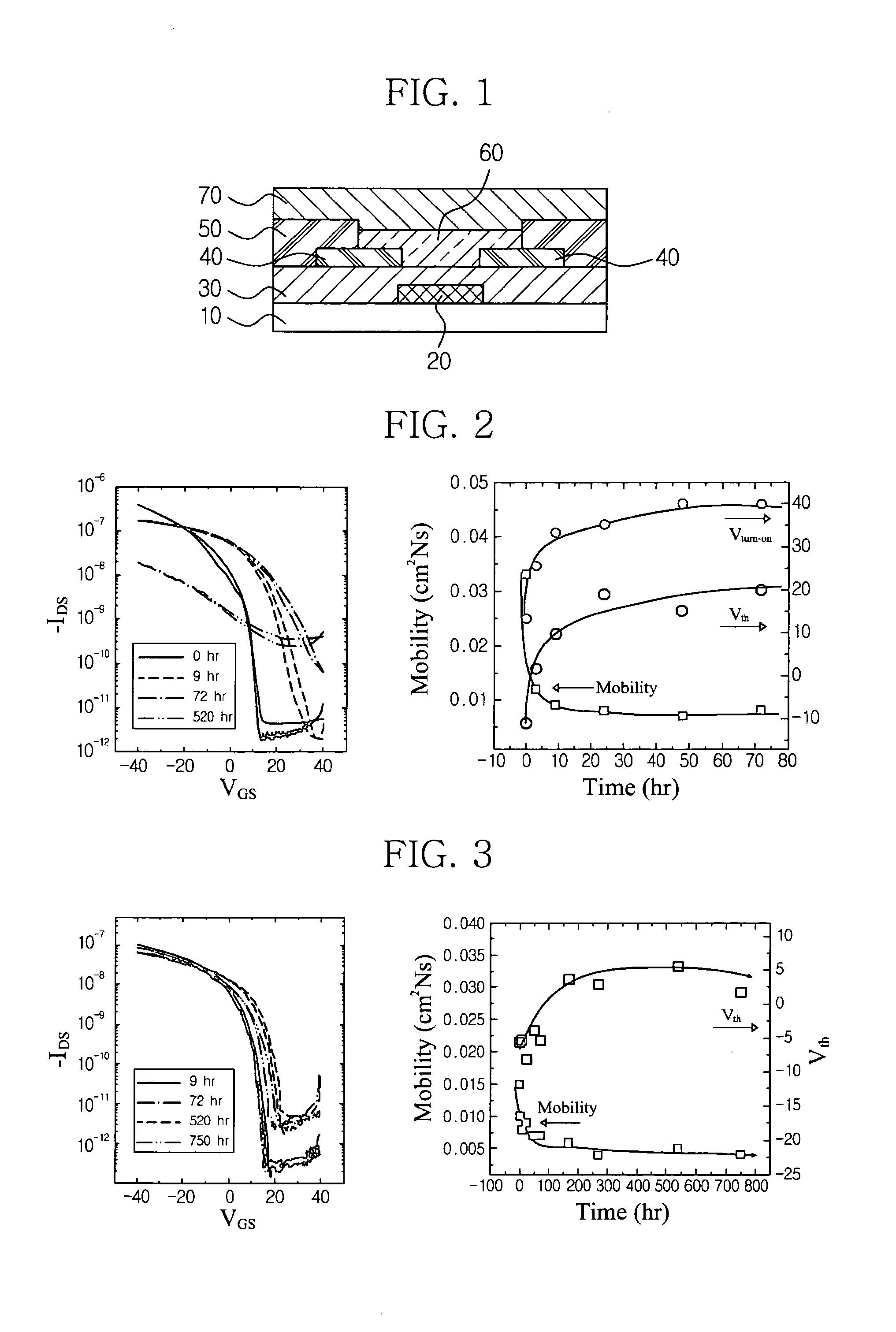
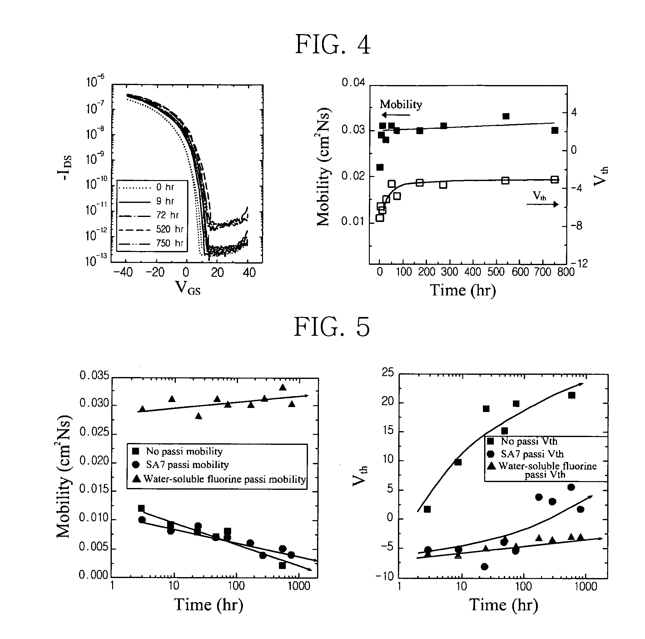
[0067]In the organic thin film transistor manufactured in Example 1 and Comparative Examples 1 and 2, in order to evaluate the electrical characteristics thereof with the change of time, the current transfer characteristics thereof were measured using a Keithley semiconductor characterization system (4200-SCS), and the results thereof were shown in FIGS. 2 to 5, respectively.

[0068]The charge mobility of the organic thin film transistor was obtained from the slope of the graph, which may be plotted with variables (ISD)1 / 2 and VG from the following Current Equation in saturation region.

ISD=WC02Lμ(VG-VT)2ISD=μC0W2L(VG-VT)slope=μC0W2LμFET=(slope)22LC0W…CurrentEquationinsaturationregion

[0069]In this Current Equation, ISD may be source-drain current, μ or μFET may be charge mobility, Co may be the capacitance of oxide film, W may be channel width, L may be channel length, VG may be gate voltage, and VT may be threshold voltage.

[0070]Threshold voltage (VT) was obtained in such a way that a...


PUM

PropertyMeasurementUnit
thicknessaaaaaaaaaa
temperaturesaaaaaaaaaa
photosensitiveaaaaaaaaaa

Abstract

Disclosed herein is a composition including a perfluoropolyether derivative, a photosensitive polymer or a copolymer thereof, and a photocuring agent, a passivation layer, organic thin film transistor, and electronic device including the same, a method of forming the passivation layer and methods of fabricating the organic thin film transistor and electronic device. The organic thin film transistor may prevent or reduce oxygen and moisture from infiltrating thereinto, and thus may prevent or reduce the degradation of the performance thereof caused by ambient air, prevent or reduce the deterioration thereof, and may more easily be formed into a pattern, thereby exhibiting characteristics suitable for use in electronics.

Description

PRIORITY STATEMENT[0001]This application claims priority under U.S.C. §119 to Korean Patent Application No. 10-2007-81939, filed on Aug. 14, 2007, in the Korean Intellectual Property Office (KIPO), the entire contents of which are incorporated herein by reference.BACKGROUND[0002]1. Field[0003]Example embodiments relate to a composition, a passivation layer, organic thin film transistor, and electronic device including the same, a method of forming the passivation layer and methods of fabricating the organic thin film transistor and electronic device, and, more particularly, to a composition which may include a perfluoropolyether derivative and a photosensitive polymer, or a copolymer thereof, a passivation layer including the composition, an organic thin film transistor including the passivation layer, an electronic device including the organic thin film transistor, method of forming the passivation layer, and methods of fabricating the organic thin film transistor and electronic de...

Claims


Application Information

Patent Timeline
Patent Type & Authority Applications(United States)
IPC IPC(8): H01L51/05G03F7/00H01L51/40C08F2/46
CPCG03F7/0046G03F7/092G03F7/038C08G65/323C08L71/00C09D171/00H01J11/40
Inventor HAHN, JUNG SEOKKIM, DO HWANKOO, BON WONLEE, SANG YOONMOON, HYUN SIK
Owner SAMSUNG ELECTRONICS CO LTD
Why Eureka
Try Eureka