Field effect transistor with gate insulation layer formed by using amorphous oxide film

a field effect transistor and amorphous oxide technology, applied in the direction of basic electric elements, electrical appliances, semiconductor devices, etc., can solve the problems of reducing the image quality of the display, affecting the operation stability of the transistor, so as to achieve good operation stability and good transistor characteristics.

Inactive Publication Date: 2009-02-19
CANON KK
View PDF8 Cites 64 Cited by
  • Summary
  • Abstract
  • Description
  • Claims
  • Application Information

AI Technical Summary

Benefits of technology

[0016]Therefore, it is the object of the present invention to provide a field effect transistor that shows good transistor characteristics and a good operation stability at the same time.
[0017]According to the present invention, the above object is achieved by providing a field effect transistor including a channel layer, a source electrode, a drain electrode, a gate insulation layer and a gate electrode formed on a substrate, characterized in that the channel layer is made of an amorphous oxide and that the gate insulation layer is made of an amorphous oxide containing Y.

Problems solved by technology

However, when Y2O3 and HfO2 are grown at low temperature, they become crystallized to produce granular agglomerates to make it difficult to form a good boundary interface between the gate insulation layer and the channel layer.
Thus, it is difficult to realize good transistor characteristics and a good operation stability at the same time.
The occurrence of hysteresis gives rise to variances in the operation of organic LED and that of liquid crystal being driven when TFTs are used e.g. in the pixel circuits of a display to consequently degrade the image quality of the display.

Method used


Image

  • Field effect transistor with gate insulation layer formed by using amorphous oxide film
  • Field effect transistor with gate insulation layer formed by using amorphous oxide film
  • Field effect transistor with gate insulation layer formed by using amorphous oxide film

Examples


example 1

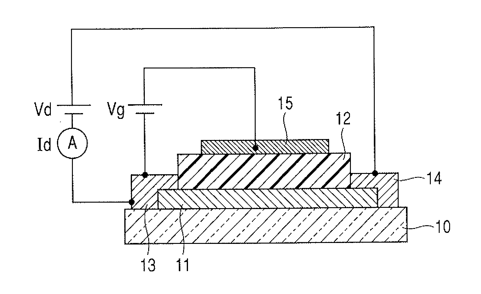
[0061]In this example, a top gate type TFT device as shown in FIG. 1A is prepared. The TFT includes a channel layer made of an In—Ga—Zn—O type amorphous oxide and a gate insulation layer made of amorphous YMnO3.

[0062]Firstly, an amorphous oxide film is formed on a glass substrate 10 (1737: tradename, available from Corning) as channel layer 11.

[0063]In this example, the In—Ga—Zn—O type amorphous oxide film is formed by high frequency sputtering in a mixture gas atmosphere of argon and oxygen. The ratio of In:Ga:Zn=1:0.9:0.6.

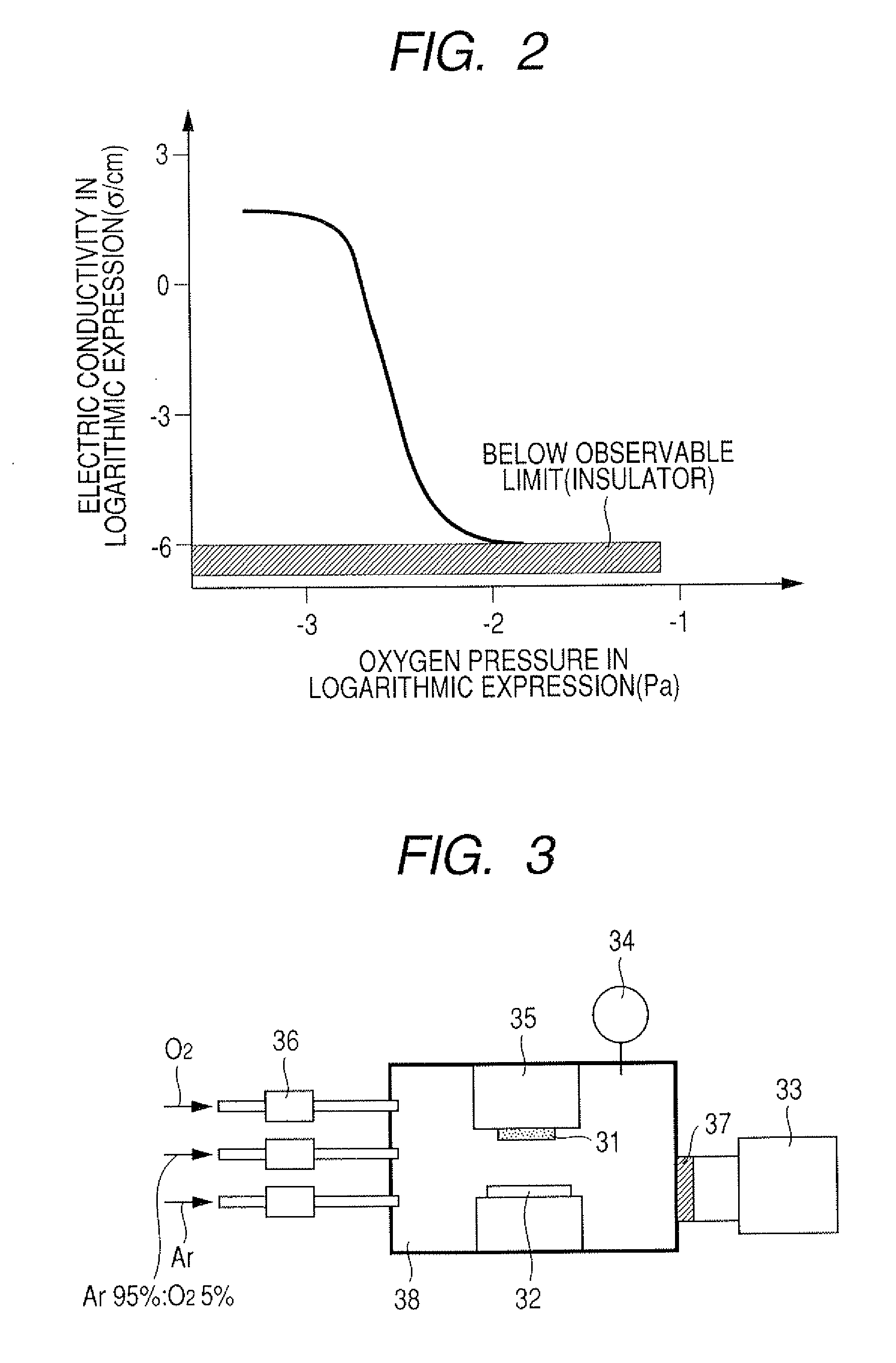
[0064]A sputtering film forming system as shown in FIG. 3 is used for forming the amorphous oxide film. In FIG. 3, there are shown a specimen (substrate) 31, a target 32, a vacuum pump 33, a vacuum gauge 34, a substrate holding unit 35, gas flow rate control units 36 provided for respective gas introduction systems, a pressure control unit 37 and a film forming chamber 38. The gas introduction systems include three systems for argon, oxygen and argon / oxygen mixtu...

example 2

[0077]In this example, a bottom gate type TFT device as shown in FIG. 1B is prepared. The TFT includes a channel layer made of an In—Ga—Zn—O type amorphous oxide and a gate insulation layer made of amorphous YMnO3 and formed at a substrate temperature of 300° C.

[0078]Firstly, a gate electrode 15 is formed to a thickness of 50 nm by using Au on a glass substrate 10 (1737: tradename, available from Corning). Photolithography and a lift-off process are used for patterning.

[0079]Then, a gate insulation layer 12 is formed to a thickness of 150 nm. The gate insulation layer 12 is a YMnO3 film prepared by means of a PLD process. The substrate temperature is set to 300° C. A process similar to that of Example 1 except the substrate temperature is used for the film formation process of the gate insulation layer. For patterning, photolithography and dry etching are also used.

[0080]Then, a channel layer of an In—Ga—Zn—O type oxide film is formed by high frequency sputtering in an atmosphere of...

example 3

[0083]In this example, a top gate type TFT device as shown in FIG. 1A is prepared on a plastic substrate.

[0084]The substrate is a polyethylene terephthalate (PET) film.

[0085]Firstly, a channel layer 11 of an In—Ga—Zn—O type oxide is formed to a thickness of 50 nm by high frequency sputtering in a mixture gas atmosphere of argon and oxygen with room temperature for the substrate temperature. The ratio of In:Ga:Zn=1:0.9:0.6. A process similar to that of Example 1 is followed for the film formation process of the channel layer. For patterning, photolithography and a lift-off process are also used.

[0086]Then, a source electrode 13 and a drain electrode 14 are formed to a thickness of 40 nm by using ITO.

[0087]For patterning, photolithography and a lift-off process are also used.

[0088]Then, a gate insulation layer 12 is formed to a thickness of 150 nm. The gate insulation layer 12 is a YMnO3 film prepared by means of a PLD process. The substrate temperature is set to room temperature. A p...


PUM


Abstract

A field effect transistor includes a channel layer 11, a source electrode 13, a drain electrode 14, a gate insulation layer 12 and a gate electrode 15 formed on a substrate 10. The channel layer is made of an amorphous oxide and that the gate insulation layer is made of an amorphous oxide containing Y.

Description

TECHNICAL FIELD[0001]The present invention relates to a field effect transistor with a gate insulation layer formed by using amorphous oxide film and also to a display apparatus.BACKGROUND ART[0002]A field effect transistor (FET) is a 3-terminal device having a gate electrode, a source electrode and a drain electrode. An FET is also an electronic active device having a functional feature of controlling the electric current flowing through the channel layer thereof and switching the electric current flowing between the source electrode and the drain electrode when a voltage is applied to the gate electrode. An FET having a channel layer formed by using a thin film that is formed on an insulator substrate such as ceramic, glass, and plastic is referred to as TFT (thin film transistor).[0003]Since a TFT is formed by means of the thin film technology, the TFT has an advantage that it can be formed on a large area substrate with ease. Because of this advantage, TFTs are being widely used...

Claims


Application Information

Patent Timeline
Patent Type & Authority Applications(United States)
IPC IPC(8): H01L29/22
CPCH01L29/7869
Inventor KAJI, NOBUYUKIYABUTA, HISATO
Owner CANON KK
Why Eureka
Try Eureka