[0006]The present invention provides a low-cost, robust, high-efficiency PV
cell that overcomes the shortcomings of the prior art by accommodating the defects of the thin-film layer, rather than attempting to eliminate them. Specifically, applicant has discovered that the performance of a thin-film PV
cell can be improved remarkably and surprisingly by increasing the resistance of the substrate to prevent defects in the thin-film layer from causing shunts. In other words, the substrate is made “fault tolerant” to accommodate the thin-film layer. This is a significant departure from conventional approaches of improving the quality of the thin films, and recognizes instead that a commercially-viable PV cell must be capable of high-volume production in which defects in the thin-film layer, such as manufacturing variances, voids, and impurities, are unavoidable as a practical matter. Furthermore, the detrimental effects of these defects would likely increase as the layer becomes thinner to enhance performance or less uniform due to high-volume manufacturing (i.e., relaxed tolerances). The substrate of the present invention, however, allows this enhanced performance and high-volume manufacturing to be realized while accommodating the associated defects.
[0007]This enhanced performance more than compensates for the reduced
voltage across the cell due to the substrate's increased resistivity. That is, although increasing the substrate's resistivity tends to diminish
voltage across the PV cell, applicant has found that significant
fault tolerance can be realized without a corresponding decrease in
solar cell voltage. Typically, substrate resistivity can be increased significantly without a precipitous decline in voltage.
[0008]In addition to
improved performance, the PV cell of the present invention also provides significant
cost savings. Specifically, the specified resistivity of the substrate generally correlates to a less pure substrate. This relatively impure subtract material is less expensive since less refining of the
semiconductor is required. For example, the desired resistivity may correspond to a
boron concentration in
silicon of greater than 10 ppm, which is relatively impure and thus readily achievable using inexpensive purification processes. Not only is the material cost low, but also the substrate can be manufactured using
casting processes, rather than complex and slow Czochralski or
Float Zone ingot formation processes. The thin-film layer also is less expensive since it can be made thinner, thus reducing
processing time and
material requirements. Additionally, the
fault tolerance of the substrate allows the thin-film layer to be formed with processes that are quicker and less expensive even though they may tend to introduce more defects (e.g., manufacturing variances / defects /
crystal boundaries) compared to traditional epitaxial vapor deposition techniques.
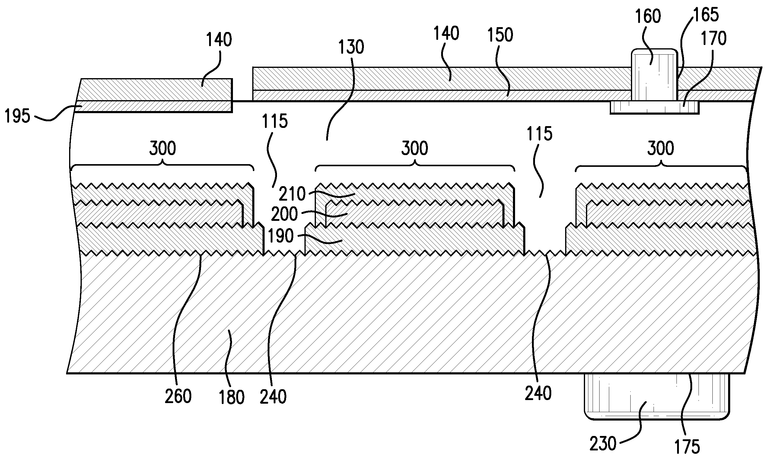
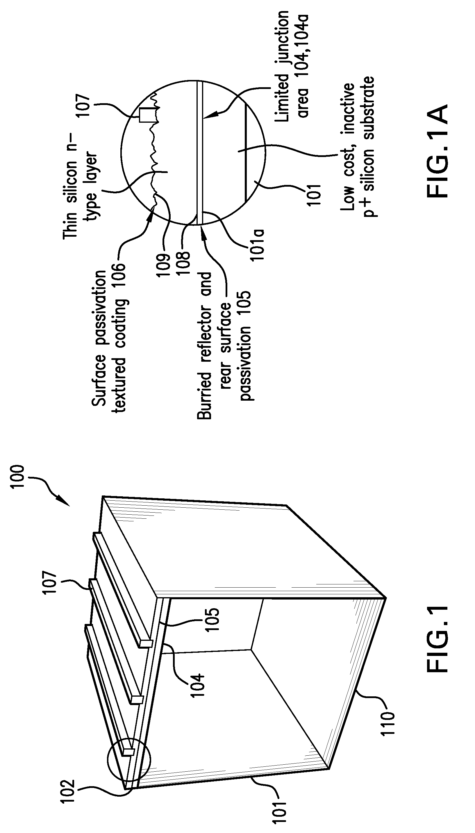
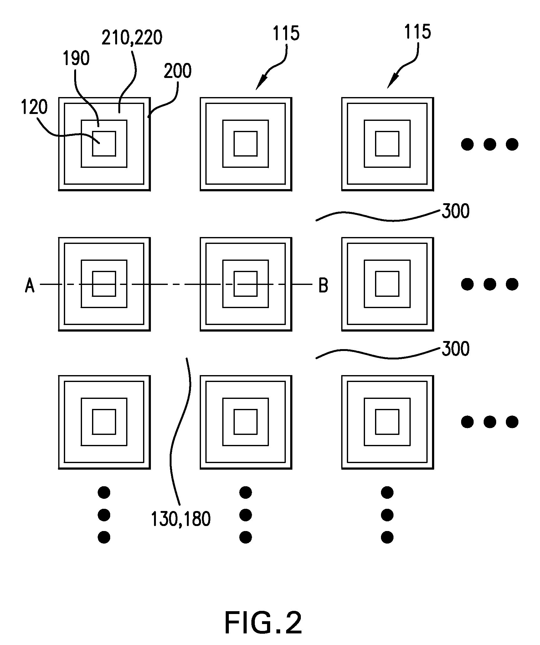
[0009]The performance of the PV cell of the present invention is further enhanced by the addition of light-capturing elements, such as reflectors and textured surfaces, and by concentrating the charge carriers using barrier
layers to reduce the size of the p-n junctions. To this end, applicant recognizes that epitaxial
lateral overgrowth (ELO) techniques, which were developed in the production of microelectronic devices, may be applied to PV cells to enable the thin-film layer to be grown over planar reflective or barrier
layers on the substrate. By using ELO processes to incorporate
reflective surfaces and other light-capturing elements into a PV cell, enhancements, such as high photogenerated currents, improved
photon conversion, and enhanced gettering potential, are synergistically realized.
[0010]Accordingly, one aspect of the present invention is a PV cell having a thin-film, epitaxially grown layer overlaying a fault resistant substrate. In one embodiment, the cell comprises a crystalline substrate having a resistivity greater than about 0.02
ohm-cm, and an
epitaxy thin-film layer on said substrate, said thin-film layer contacting said substrate in at least one region to define a p-n junction. In one embodiment, the PV cell has improved efficiency through the use of reflectors and other light capturing
optics. For example, reflectors between the substrate and the thin-film layer improve the conversion of photons to charge carriers which can be transported across the p-n junction.

