
Light emission device

Active Publication Date: 2009-03-05
SEOUL SEMICONDUCTOR
View PDF6 Cites 49 Cited by
  • Summary
  • Abstract
  • Description
  • Claims
  • Application Information

AI Technical Summary

Benefits of technology

[0019]In the light emitting apparatus according to the present invention, the ceramic phosphor having a predetermined transparency with respect to a using light having a wavelength is used, so that the light emitted from an inner portion of the phosphor can be effectively extracted to outside of the light emitting apparatus without being absorbed or scattered by an opaque phosphor powder, even if there is used a phosphor having a large thickness enough to sufficiently absorb the light emitted from the semiconductor light emitting element.
[0097]As described above, according to the light emitting apparatus of the present invention, it becomes possible to provide a light emitting apparatus having a high luminous efficiency and an excellence in industrial productivity. In addition, all of the constituting parts including the phosphor can be formed in a solid state, an industrial production efficiency of the light emitting apparatus can be remarkably improved.

Problems solved by technology

However, since the powdery phosphor used in the above conventional light emitting apparatus was opaque, the light emitted from an inner portion of the phosphor layer formed by piling up the phosphor powders was disadvantageously absorbed and scattered by the opaque phosphors located at outside the outstanding phosphor.
As a result, it was difficult to effectively extract the emitted light to outside the light emitting element.
On the other hand, in a case where the thickness of the phosphor layer is increased to be thick for the purpose of allowing the phosphor layer to sufficiently absorb the light emitted from the semiconductor light emitting element, the light extraction efficiency of extracting the light emitted from the phosphor is also disadvantageously lowered, so that there had been posed a problem of lowering the entire light extracting efficiency of the light emitting apparatus.
Further, in a case where a semiconductor light emitting element for emitting ultraviolet light is used, the resin mixed with the phosphor powder was liable to be deteriorated by the ultraviolet light, so that there had been posed a problem that a life duration of the light emitting apparatus was disadvantageously limited and the durability of the light emitting apparatus was also lowered.
Furthermore, in production lines of a light emitting apparatus formed by using a dip method, there was a difficulty of that a processing time required until the resin was cured was long, so that a mass-productivity of the light emitting apparatus was disadvantageously lowered.
However, a difference in specific gravity between the resin and the phosphor powder is large, so that a management of the concentration of the phosphor is difficult.
As a result, there has been also posed a problem that the concentration of the phosphor becomes uneven for the respective operations of injecting the phosphor.
Furthermore, an injection amount of a resin suspension of the phosphor with respect to each of the light emitting apparatus is extremely small to be 0.1 mcc or less, so that it was extremely difficult to accurately control such a small amount so as to have a predetermined value in a level of mass-production process.
As a result, there has been arisen a problem that the injection amount and a content of the phosphor are greatly fluctuated, so that the color tone of the light emitted from the light emitting apparatus is not uniform.
In this case, however, the concentration of the phosphor is low and a sufficient emission output could not be obtained.
In addition, in this case, when the concentration of the phosphor is increased, there has been arisen a problem to be technically solved such that a transparency of the resin layer containing the phosphor is lowered thereby to decrease the emission output.

Method used


Image

  • Light emission device
  • Light emission device
  • Light emission device

Examples


example 1

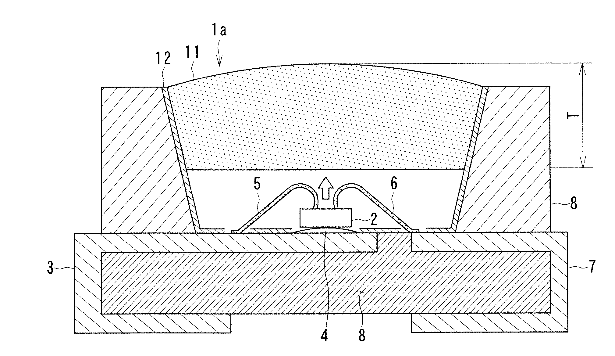
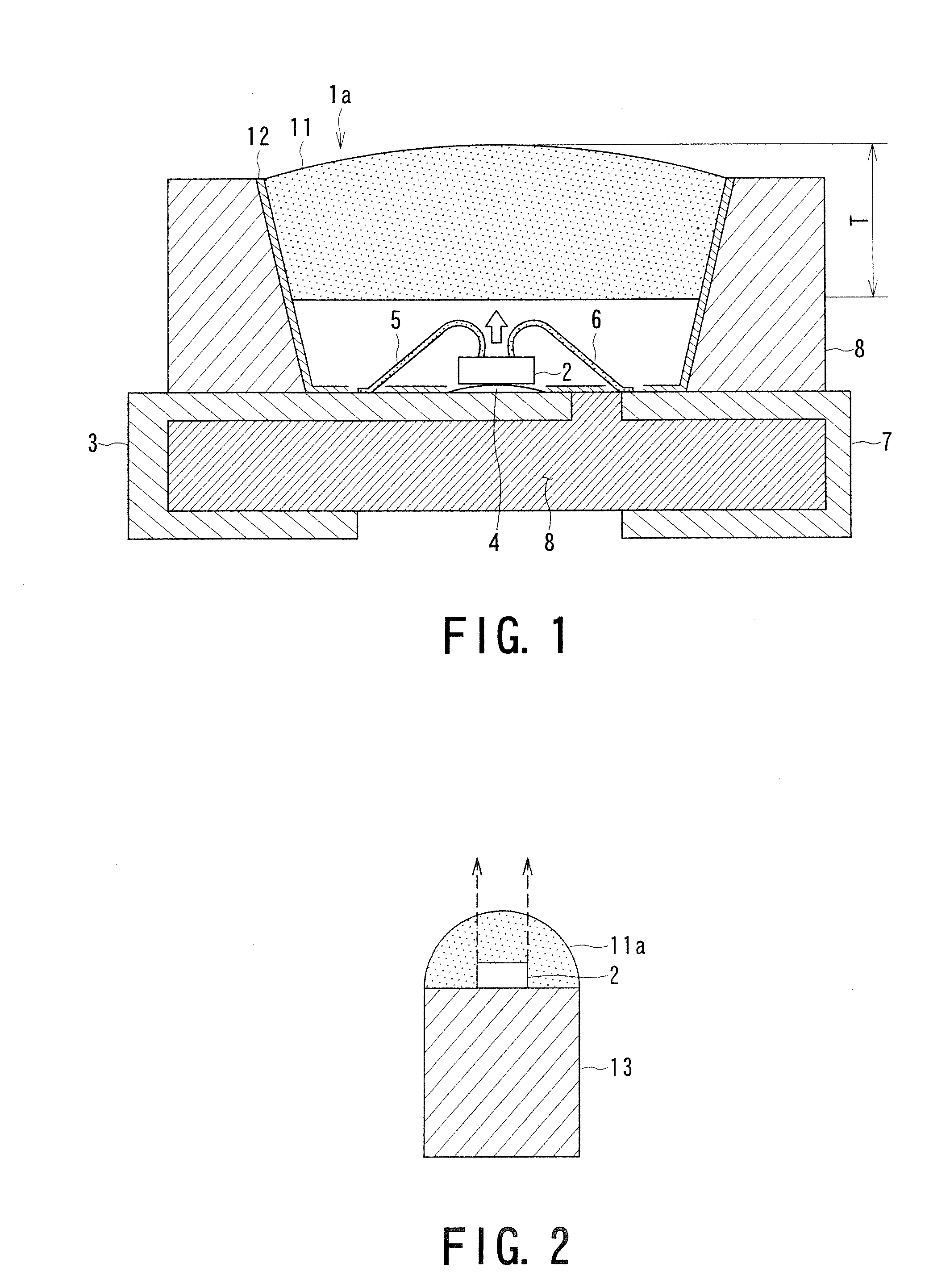
[0062]0.9 mol of strontium carbonate, 0.08 mol of barium carbonate, 0.02 mol of calcium carbonate, 0.001 mol of europium oxide and 0.5 mol of silica were weighted to prepare a phosphor material. Then, ammonium chloride was added to the phosphor material at an amount of 2 mass % with respect to the phosphor material and the phosphor material was sufficiently blended thereby to prepare a material mixture. Next, the material mixture was injected into a crucible made of alumina and the material mixture was calcined in air atmosphere under the temperature condition of 600° C. for one hour. After cooling the crucible, the calcined material was well mixed. Subsequently, the mixture was injected into the alumina crucible, and then sintered in a reductive atmosphere composed of 3%-hydrogen gas and nitrogen gas at a temperature condition of 1200° C. for two hours. Thus obtained sintered body was then pulverized, followed by wet-cleaning and drying. The dried material was passed through a siev...

examples 2-4

[0070]The same manufacturing process as in Example 1 was repeated except that only a thickness of the sintered body of the circular-plate-shaped ceramic phosphor 11 prepared in Example 1 was changed as shown in Table 1. Each of the ceramic phosphors 11 was attached to a central portion of a bottom surface of a packaging container, thereby to prepare respective light emitting apparatus of Examples 2-4 each having the same structure as in Example 1 shown in FIG. 1.

[0071]With respect to each of thus prepared light emitting apparatuses 1a, an emission output and an emission chromaticity were measured at a time when an electric power was inputted under the same conditions as in Example 1, thereby to obtain results shown in Table 1 hereunder.

TABLE 1Thickness ofEmissionCeramic PhosphorEmission OutputChromaticitySample No.(Sintered Body) (mm)(mCd / m2)(x, y)Example 20.66500.31, 0.30Example 30.86800.33, 0.34Example 41.07000.35, 0.36

[0072]As is clear from the results shown in Table 1, according...

example 5

[0075]The same manufacturing processes of material mixing, molding and sintering as in Example 1 were repeated under the same conditions in Example 1 except that the ratio of the europium oxide to be contained in the phosphor material was changed to 0.004 mol, thereby to prepare a circular-plate-shaped ceramic phosphor as a sintered body.

[0076]A density (relative density) of this sintered body with respect to a true specific gravity was 99.8%, while a transmission of a light having wavelength of 570 nm was 40% and a transmission of a light having wavelength of 395 nm was 2%. In addition, a surface roughness Ra of each of upper and lower surfaces of the circular-plate-shaped ceramic phosphor was 50 μm.

[0077]On the other hand, a flip chip type semiconductor light emitting diode having an emission peak wavelength of 395 nm and an outer size of 200 μm×200 μm was prepared, and there was prepared a packaging container having a diameter of 2 mm and a white-colored reflecting member 12 prov...


PUM


Abstract

A light emitting apparatus 1 comprises: a semiconductor light emitting element 2; and a transparent ceramic phosphor 11 for converting a wavelength of a light emitted from the semiconductor light emitting element 2, wherein the semiconductor light emitting element 2 emits an ultraviolet light, and the ceramic phosphor 11 corresponding to the semiconductor light emitting element 2 has: a minimum transmission of 0.1 to 40% under a wavelength of 350-420 nm; and a transmission of 10 to 90% under an emission peak wavelength of the ceramic phosphor.

Description

TECHNICAL FIELD[0001]The present invention relates to a light emitting apparatus in which a light emitted from a light emitting diode is subjected to a wavelength conversion by a ceramic phosphor thereby to irradiate the light to outside. More specifically, the present invention relates to a light emitting apparatus having a high light-extraction efficiency of extracting the light emitted from the ceramic phosphors and is excellent in luminescence intensity.BACKGROUND ART[0002]A light emitting diode (LED) is a semiconductor diode for radiating light, and has a function of converting an electrical energy into visible light or ultraviolet light. Particularly, for the purpose of utilizing the visible lights, there has been widely used as LED lamp in which a semiconductor light emitting element (light emitting chip) formed of light emitting materials such as GaP, GaAsP, GaAlAs or the like is sealed by a transparent resin or the like. Further, there has been also widely used as light emi...

Claims


Application Information

Patent Timeline
IPC IPC(8): H01L33/00H01L33/50
CPCH01L33/502H01L2224/48091H01L2224/73265H01L2924/00014
Inventor OKAMURA, MASAMITAMATANI, MASAAKISHIDA, NAOMIOOTSUKA, KAZUAKIFUKUTA, YUKIHIRO
Owner SEOUL SEMICONDUCTOR
Features
  • Generate Ideas
  • Intellectual Property
  • Life Sciences
  • Materials
  • Tech Scout
  • Unparalleled Data Quality
  • Higher Quality Content
  • 60% Fewer Hallucinations
Learn More