Hybrid photovoltaically active layer and method for forming such a layer

a photovoltaic active and hybrid technology, applied in the field of solar cells, can solve the problems of high rate of recombination of photo-generated carriers, high photovoltaic efficiency, and large market response, and achieve high power dc pulsing, enhance excitation and oscillation rate, and increase the effect of tim

Inactive Publication Date: 2009-03-12
SUB ONE TECH
View PDF11 Cites 8 Cited by
  • Summary
  • Abstract
  • Description
  • Claims
  • Application Information

AI Technical Summary

Benefits of technology

[0011]The process that is well suited for forming the photovoltaically layer in accordance with the invention employs the hollow cathode effect and high power DC pulsing. The pulse duration is a particularly important factor. Longer pulses increase the amount of time for the silicon atoms to establish their energetically preferred locations. Nevertheless, the time between two high powered DC pulses is not less than the duration of each pulse. An example of a PIN solar cell junction formed using this method is as follows: a hollow cathode chamber containing the solar cell substrate (e.g., a stainless steel foil) is heated in hydrogen at a 50% duty cycle. A p-type junction may be formed using silane and 2% diaborane (or other p-type dopant), followed by an intrinsic silicon layer (typically the layer of focus with respect to the present invention). Two frequencies can be used for power application to the plasma, with the higher frequency pulsing preferably being at 25 kHz and a 50% duty cycle. The lower frequency “burst” at 25 Hz can be run (but may be deleted in some embodiments) at a 10% duty cycle for a total duty cycle of 5%. High current per pulse is used for the higher frequency pulsing, such as a current in the range of 25 mA / 2.54 cm2 to 100 mA / 2.54 cm2, (e.g., a 25 kHz pulse at 60 mA / 2.54 cm2). Following this, the n-type layer may be formed using silane and 2% phosphine (or other n-type dopant) in hydrogen. Preferably, the pulse duration is within the range of 5% to 50% of the cycle. As one possibility, 1,000 volt pulses (20 W / cm2) have a 10 microsecond “on” time and 90 microsecond “off” time, yielding a morphology which has the correct regime, according to TEM evaluation (transmission electron microscopy).
[0012]The “hollow cathode effect” as used herein. In case a large increase in current as compared to convention plasma glow. The increase is due to the “oscillation motion” of fast (hot, accelerated) electrons between opposite space charge sheaths, which enhances the excitation and oscillation rates in the plasma several times higher than the conventional glow discharge. Because this electron pendulum motion is related to the mean free path of the fast electrons, there is a relationship of the hollow cathode effect to pressure within the hollow cathode and the spacing between the two or more electrodes. That is, a hollow cathode with a small spacing will operate at a higher pressure than a hollow cathode with a larger spacing.
[0013]While the fabrication of one or more photovoltaically active layer in accordance with the invention may take place within a tube, the end product need not be tubular. For applications in which the layer is formed within a cylindrical workpiece, the workpiece may be cut into sections which then are used to generate solar energy. Arcs of 120 degrees to 180 degrees substantially increase the collected solar power when exposed diffused light, such as in cloudy or hazy conditions.
[0014]In another embodiment, the photovoltaically active layer is formed on a substrate that is progressed through an area in which the proper deposition conditions are established. For example, a flexible substrate may be progressed through one or more tubes in which a hollow cathode effect is established. The substrate may temporarily or permanently cover the wall of the tube. Alternatively, the substrate may cover only a portion of the tube wall, such as a spiraling substrate that is progressed through the tube.

Problems solved by technology

However, the current state of the art solar cell manufacturing technology employs large inexpensive PECVD machines.
Despite the low photovoltaic efficiency, solar cell production technology has reached a price-point threshold that triggers large market response.
However, while absorptivity is an important requirement for low cost solar cells, conventional atomic disorder also result in a high rate of recombination of photo-generated carriers.
This is significant, since the increase in layer thickness increases the overall expense of a solar cell.

Method used


Image

  • Hybrid photovoltaically active layer and method for forming such a layer
  • Hybrid photovoltaically active layer and method for forming such a layer
  • Hybrid photovoltaically active layer and method for forming such a layer

Examples


Embodiment Construction

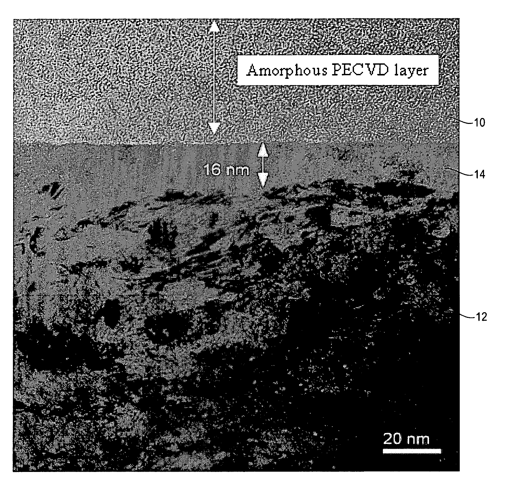
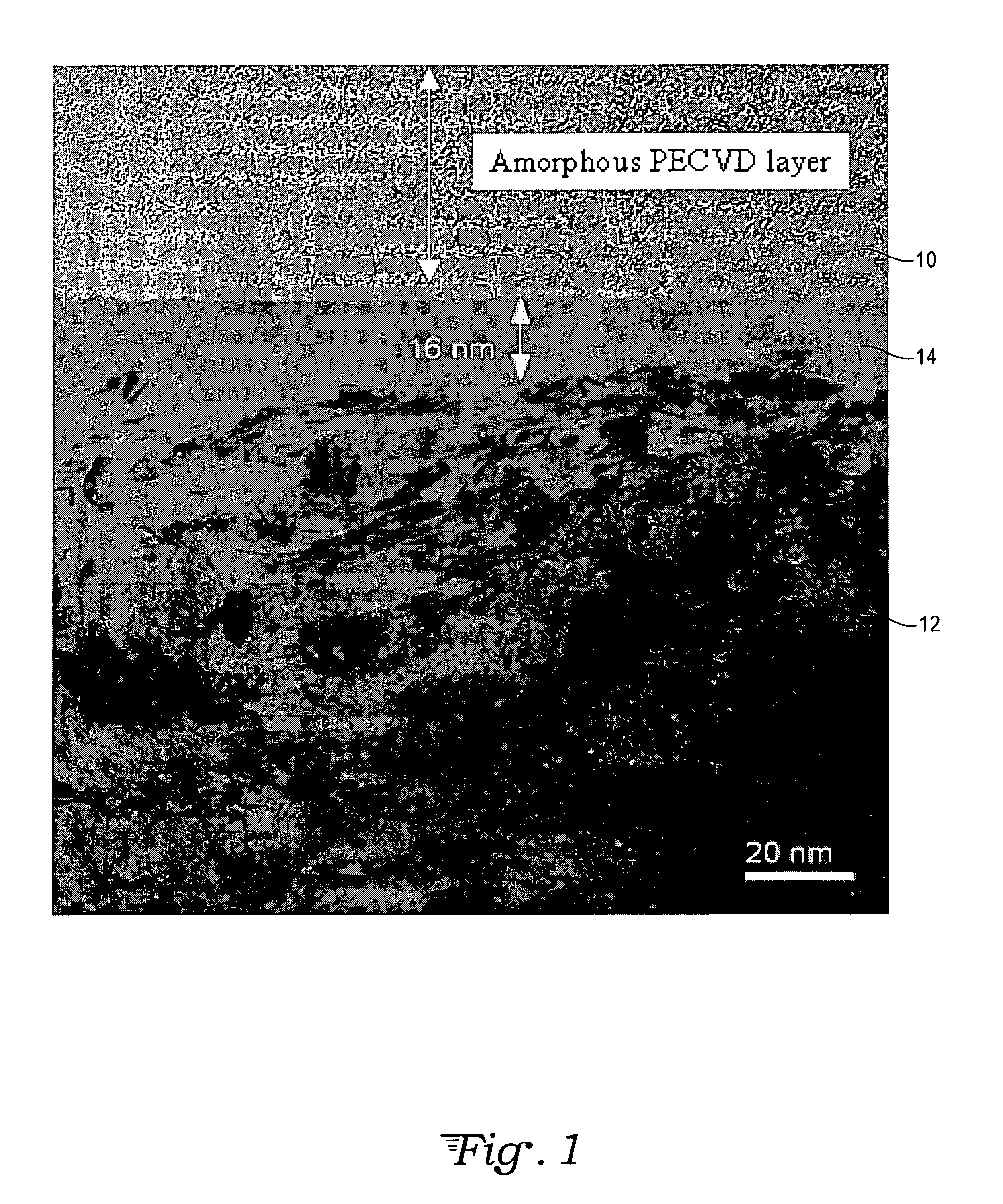
[0021]FIG. 1 shows an a-Si:H layer 10 formed on a steel substrate 12. The a-Si:H layer was formed using PECVD techniques. Additionally, the deposition of this layer occurred after establishing a hollow cathode effect within a deposition chamber, such as described in U.S. Pat. No. 7,300,684 to Boardman et al. and U.S. Patent Publication No. 2008 / 002994 to Tudhope et al., both of which are assigned to the assignee of the present invention. In relating the description of these two patent documents to the formation shown in FIG. 1, the steel substrate 12 is a workpiece in which the hollow cathode effect is established. Since the electron mean-free path is related to the inner diameter of the workpiece, the proper pressure setting will cause high energy electrons to oscillate between electron walls and an increase in ionizing collisions will occur. In establishing this condition, pressure must be decreased as the diameter of the workpiece is increased. As one possibility, a 25 millimeter...


PUM

PropertyMeasurementUnit
frequencyaaaaaaaaaa
frequencyaaaaaaaaaa
pressureaaaaaaaaaa

Abstract

A “hybrid” photovoltaically active layer is homogenous (in a direction parallel to the major surfaces of the layer) with respect to film constituents, but is non-homogenous with respect to photovoltaic properties. First regions exhibit high absorptivity, while second regions that are perpendicular to the major surfaces of the layer exhibit a higher carrier mobility. The method for forming the layer includes one or all of chemical vapor deposition, the hollow cathode effect, and high power DC pulsing.

Description

CROSS-REFERENCE TO RELATED APPLICATION[0001]This application claims priority from U.S. provisional application Ser. No. 60 / 993,567, filed Sep. 12, 2007.TECHNICAL FIELD[0002]The present invention relates generally to solar cells and more particularly to methods and apparatus for fabricating solar cells.BACKGROUND ART[0003]Silicon is the most commonly used component for forming a photovoltaically active material, since silicon is abundant, inexpensive, and environmentally responsible. Of the various forms of silicon, hydrogenated amorphous silicon (a-Si:H) film deposited by plasma enhanced chemical vapor deposition (PECVD) is the least expensive used in fabricating solar cells. However, the current state of the art solar cell manufacturing technology employs large inexpensive PECVD machines.[0004]Despite the large capital equipment requirements, an a-Si:H layer that is formed using conventional processing by material properties which limit photovoltaic efficiency to approximately 10%,...

Claims


Application Information

Patent Timeline
Patent Type & Authority Applications(United States)
IPC IPC(8): H01L31/00B01J19/08
CPCC23C16/04Y02E10/547C23C16/503C23C16/515C23C16/54H01J37/32018H01J37/32027H01L31/03685H01L31/03762H01L31/0747H01L31/075H01L31/1804Y02E10/548Y02E10/545C23C16/24Y02P70/50
Inventor UPADHAYAYA, DEEPAKBOARDMAN, WILLIAM J.DORNFEST, CHARLES
Owner SUB ONE TECH
Why Eureka
Try Eureka