Semiconductor memory device and manufacturing method therefor

a memory device and semiconductor technology, applied in semiconductor devices, capacitors, electrical devices, etc., can solve the problems of difficult to ensure a sufficient storage capacitance, high cost, and difficulty in microfabrication such as dry etching, so as to reduce the mechanical strength of such a structure, prevent the breakage of capacitor electrodes, and reduce the cos

Inactive Publication Date: 2009-03-26
LONGITUDE LICENSING LTD
View PDF2 Cites 22 Cited by
  • Summary
  • Abstract
  • Description
  • Claims
  • Application Information

AI Technical Summary

Benefits of technology

[0032]A first advantage is that microfabrication such as dry etching becomes easier because an aspect ratio of capacitors in respective layers can be kept low and large capacity of capacitors can be obtained according to a simple manufacturing method because capacitor electrodes can be restrained from being broken. Thus, a DRAM with high integration degree beyond the conventional limit of microfabrication can be attained.
[0033]A second advantage is that a refresh cycle of a DRAM can grow longer to reduce power consumption because capacitors having great capacitance can be easily formed by stacking capacitor layers as required. Specifically, by increasing the charge quantity capable of being...

Problems solved by technology

However, further development of miniaturization requires formation of a capacitor with desired capacitance on a memory cell of smaller size and therefore the mechanical strength of such a structure will be lowered and the difficulty in performing microfabrication such as dry etching has become high and hence it has become difficult to ensure a sufficient storage capacitance.
In the method of Japanese Patent Application Laid-Open No. 2003-197771, it will be caused a problem on ...

Method used


Image

  • Semiconductor memory device and manufacturing method therefor
  • Semiconductor memory device and manufacturing method therefor
  • Semiconductor memory device and manufacturing method therefor

Examples


first exemplary embodiment

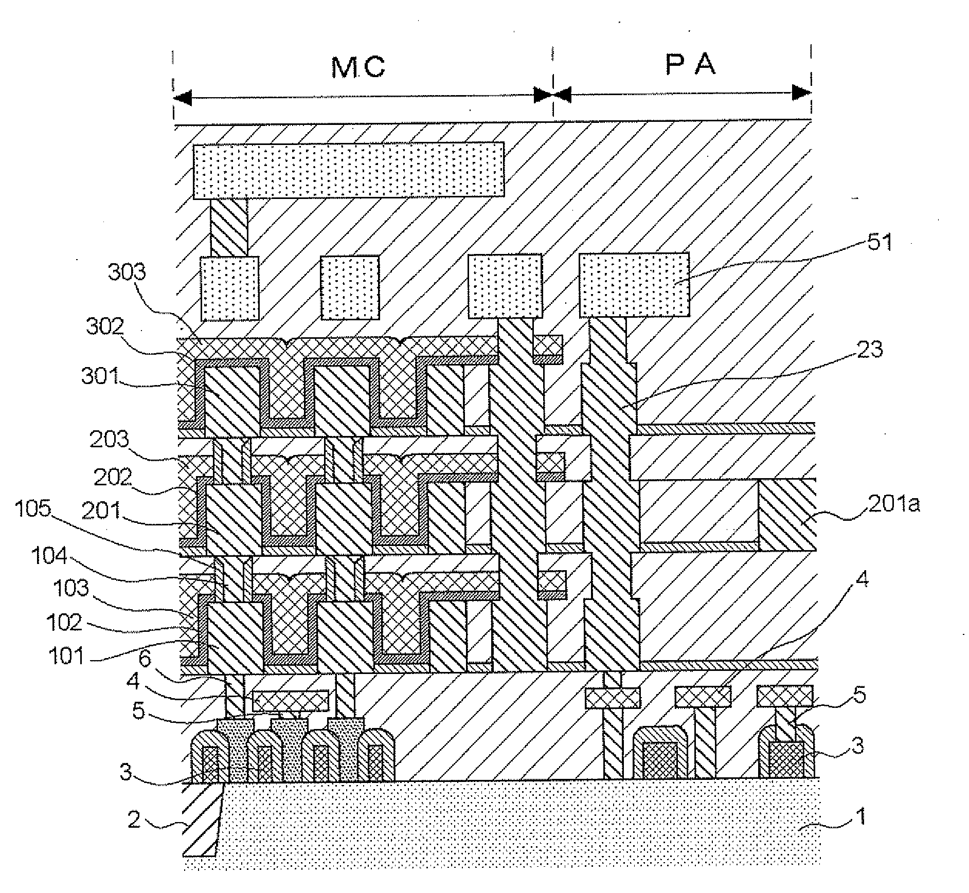
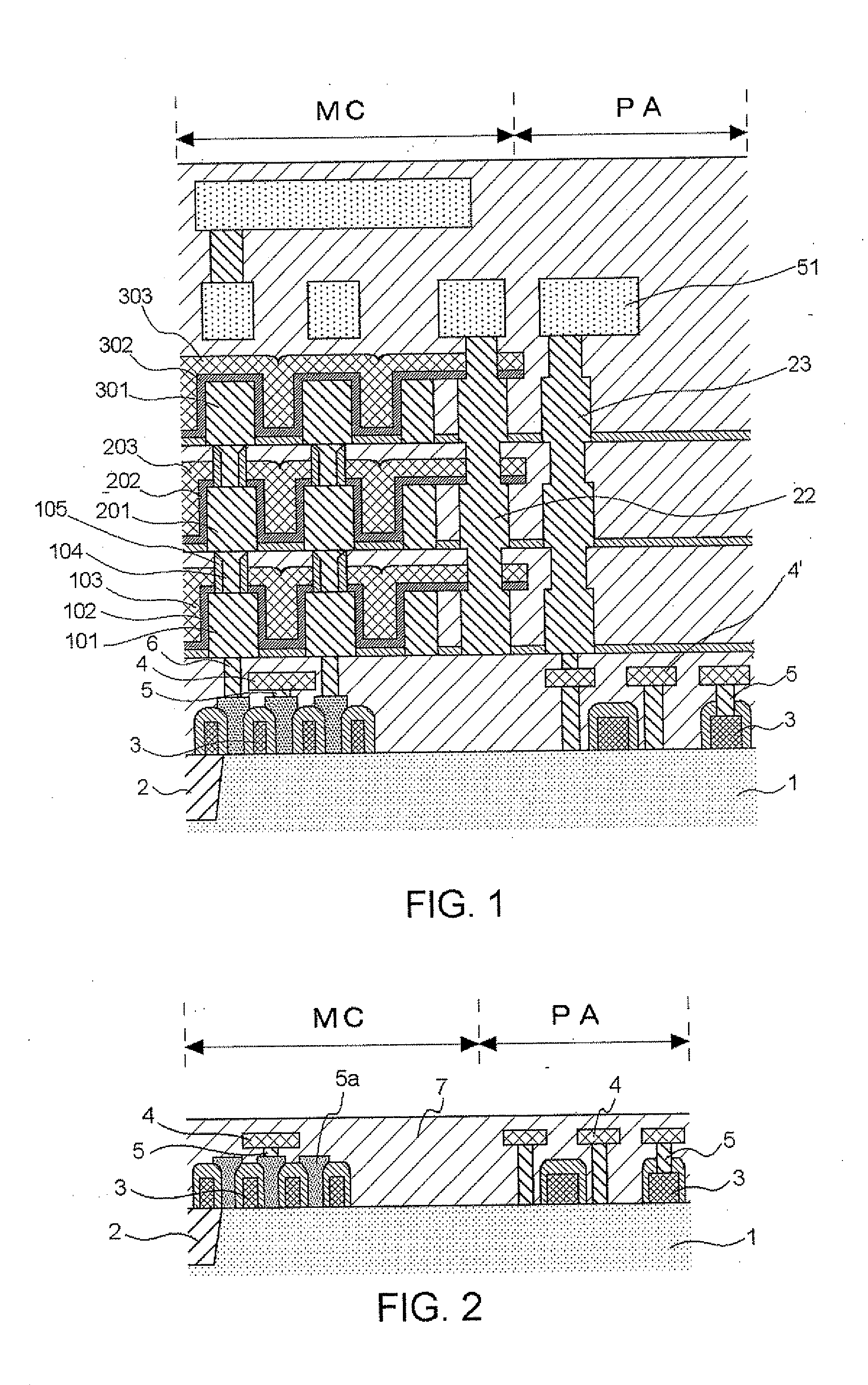
[0040]FIG. 1 illustrates a sectional schematic view of a DRAM as a first exemplary embodiment of the present invention. In FIG. 1, memory cell area (MC) is illustrated on the left side and a peripheral circuit area (PA) is illustrated on the right side.

[0041]In the same way as a conventional DRAM, on silicon substrate 1, there are provided element isolation region 2, a gate insulation film (not illustrated because of small thickness) of a MOS (Metal-Oxide-Semiconductor) transistor, gate electrode (word line) 3, bit line 4 and contact plug 5 for interconnecting thereof. Bit line 4 functions as a wiring layer for connecting respective transistors in the peripheral circuit region.

[0042]In the memory cell area, cylindrical or prismatic first capacitor lower electrodes 101 are provided so as to be connected to silicon substrate 1 through contact plug 6. The surface of each of lower electrodes 101 is covered with first capacitor insulation film 102 and further first upper electrode 103 is...

second exemplary embodiment

[0074]In the first exemplary embodiment described above, an upper electrode and a contact plug may be formed for each capacitor layer, using a specific photo mask. Accordingly, a local wiring is formed between capacitor upper electrodes in respective layers and a contact plug allows the local wirings to be connected with each other and therefore multilayering of local wirings can be achieved.

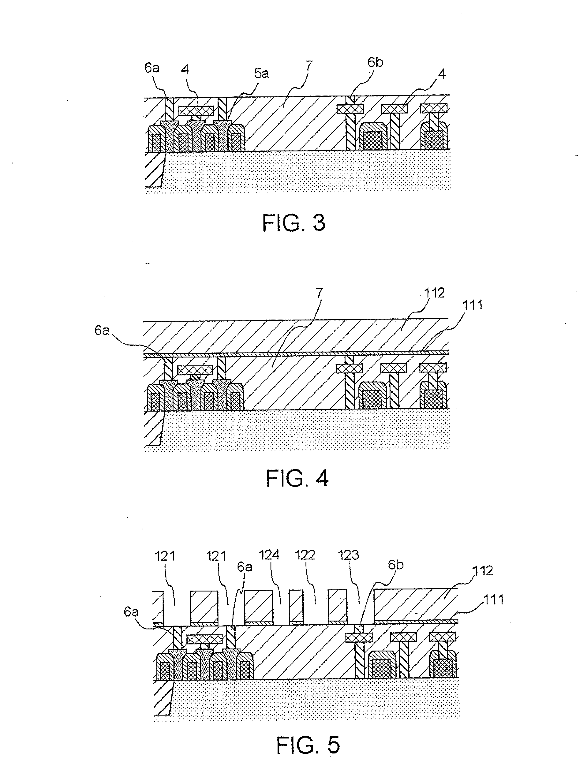
[0075]FIG. 17 illustrates a sectional view of wiring layer 203a formed in the peripheral circuit area (PA) using the same layer as upper electrode 203 at the second layer from the bottom.

[0076]Capacitor insulation film 202 is patterned in the same way and is left as 202a under wiring layer 203a, but no particular problems occur. For connection of wiring layer 203a with another wiring positioned at the upper or lower layer, a contact plug may be provided as needed. Accordingly, in a peripheral circuit area, the same layer as the upper electrode of a capacitor at each layer can be used as a local ...

third exemplary embodiment

[0077]In the first exemplary embodiment described above, a contact plug portion may be formed into a dual damascene structure using a specific photo mask for each capacitor layer. In the second exemplary embodiment described above, the same layer as an upper electrode of each capacitor has been used as a local wiring layer. On the other hand, in the present embodiment, a wiring layer is formed in the same layer as the lower electrode. Specifically, in the peripheral circuit area, a groove pattern for wiring is formed at the same time when an opening for embedding a lower electrode is formed. Furthermore, in the peripheral circuit area, a contact hole for connecting the local wiring with the lower wiring layer is formed using the dual damascene method. Subsequently, by burying a conductor for a lower electrode of a capacitor, a local wiring layer for a peripheral circuit area and a contact plug can be formed at the same time.

[0078]FIG. 18 illustrates a sectional view in which wiring ...


PUM


Abstract

A semiconductor memory device in which a plurality of capacitors each including a columnar lower electrode, a capacitor insulation film and an upper electrode are stacked with interlayer films therebetween, a contact plug connects an upper face of each lower electrode of a lower layer with a bottom face of each lower electrode of an upper layer, and another contact plug connects upper electrodes of the capacitors in respective layers with each other.

Description

BACKGROUND OF THE INVENTION[0001]1. Field of the Invention[0002]The present invention relates to a semiconductor memory device and a manufacturing method therefor, and more particularly to a structure of a capacitor with a desired capacitance on a miniaturized memory cell and a manufacturing method therefor.[0003]2. Description of Related Art[0004]In a semiconductor memory device (Dynamic Random Access Memory, hereinafter referred to as “DRAM”) which allows writing and reading as needed, one capacitor is connected with one transistor to retain charges. With recent technological development, there has become commercially practical a semiconductor memory device using a capacitor of a three-dimensional structure, among semiconductor memory devices such as, especially, a DRAM. For example, a conventional semiconductor memory device illustrated in FIGS. 11 and 12 of Japanese Patent Application Laid-Open No. 2000-156479 uses a cylindrical-type capacitor structure. For high integration deg...

Claims


Application Information

Patent Timeline
IPC IPC(8): H01L29/94H01L29/00H01L21/20
CPCH01L27/0688H01L28/40H01L27/10897H01L27/10894H10B12/50H10B12/09
Inventor YOKOI, NAOKI
Owner LONGITUDE LICENSING LTD
Why Eureka
Try Eureka