Non-polar iii-v nitride semiconductor and growth method

Active Publication Date: 2009-03-26
IQE
View PDF46 Cites 70 Cited by
  • Summary
  • Abstract
  • Description
  • Claims
  • Application Information

AI Technical Summary

Benefits of technology

[0010]The current invention is directed to method of producing non-pol

Problems solved by technology

Consequently, when using these conventional materials the radiative recombination time increases at the expense of quantum efficiency and a red-shift of the emission occurs.
However, the use of non-polar III nitride materials for semiconductor devices, such as high current density drive light-emitting diodes (LEDs) and laser diodes (LDs), may disrupt the current trend for polar materials.
Unfortunately, this technology suffers from a low growth rate and is limited to s

Method used


Image

  • Non-polar iii-v nitride semiconductor and growth method
  • Non-polar iii-v nitride semiconductor and growth method
  • Non-polar iii-v nitride semiconductor and growth method

Examples


example 1

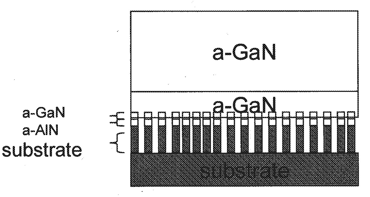
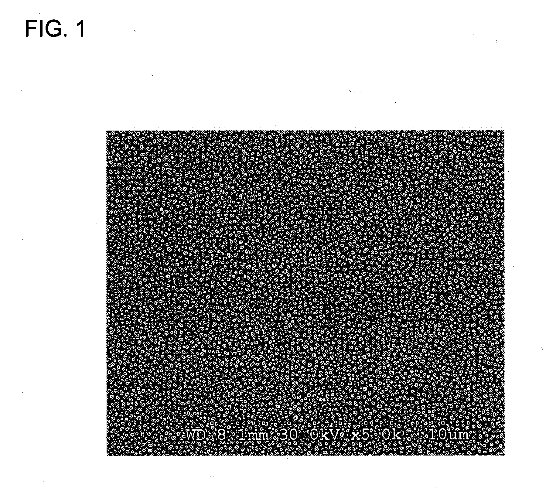
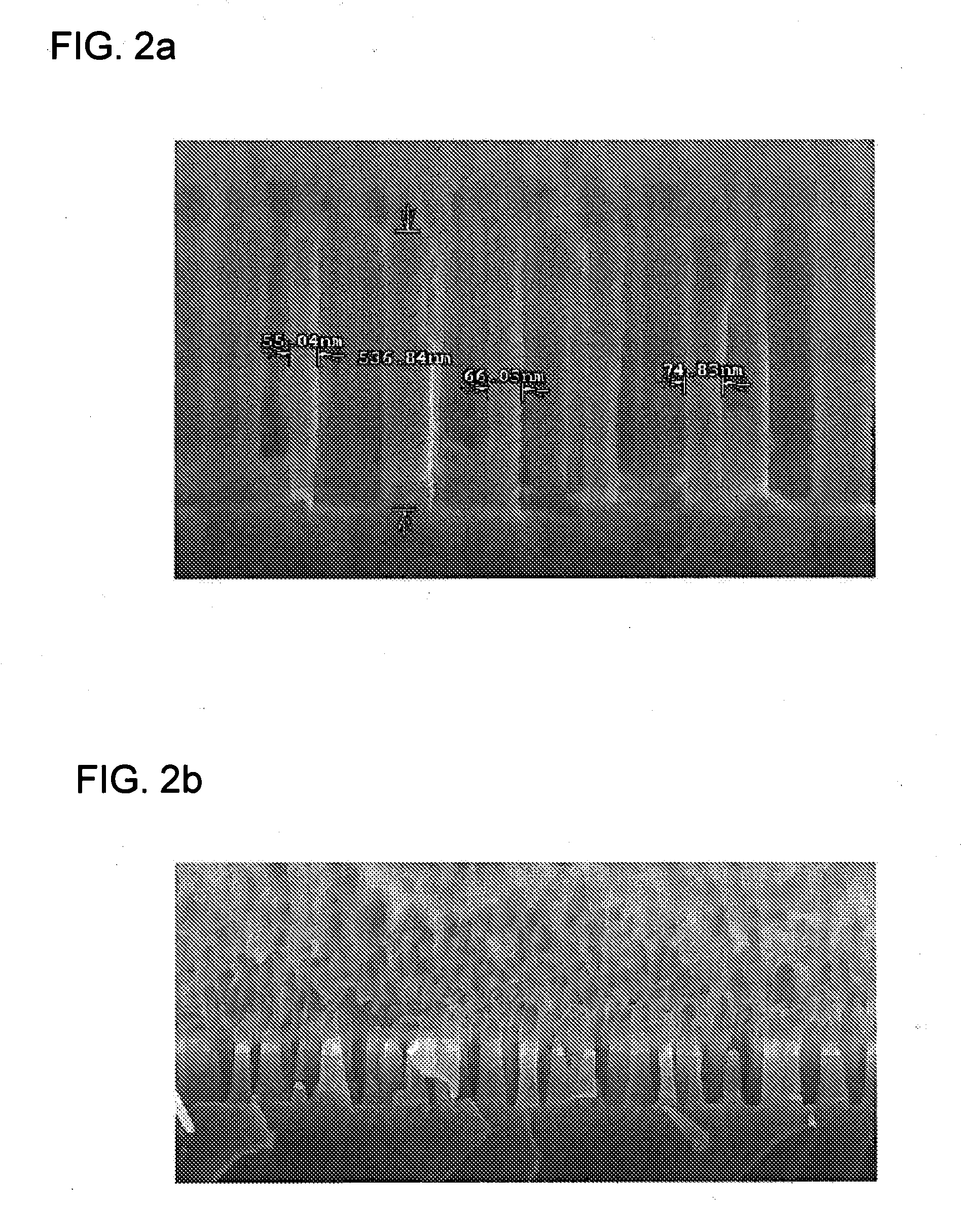
[0084]A γ-plane-oriented sapphire substrate of about 2 inches (5.08 cm) in diameter with MOCVD-deposited a-plane AlN (20 nm) and GaN of about 0.6 μm is loaded onto the substrate holder of a HVPE vertical reactor. Before loading, the a-plane GaN template is degreased in KOH for a few seconds, rinsed in de-ionized water, etched in a H2SO4 / H3PO4=3:1 solution at 80° C. for a few minutes, then rinsed in de-ionized water. It is then necessary to create a mask onto the template. Firstly, a thin dielectric layer of SiO2 or Si3N4 of ˜200 nm is deposited by PECVD onto the GaN template. Then, a thin Ni metal layer of 2-30 nm is deposited by e-beam evaporation or sputtering onto the dielectric layer. Rapid annealing of the metal under N2 gas at an ambient temperature of ˜830° C. for about one minute is carried out to form a high density of Ni nano-dots, as shown in FIG. 1, forming the nano-mask. The thickness of the Ni metal allows the control of the density and the dimension of the Ni nano-dot...

example 2

[0092]This Example is similar to Example 1, except that here the a-plane GaN nanocolumns are made using anodic porous alumina nano-mask fabrication processes. A γ-plane-oriented sapphire substrate of about 2 inches (5.08 cm) in diameter with MOCVD deposited a-plane AlN (20 nm) and GaN of 0.6 μm is loaded onto the substrate holder of the HVPE vertical reactor. Before loading, the a-plane GaN template is degreased in KOH for a few seconds, rinsed in de-ionized water, etched in a H2SO4 / H3PO4=3:1 solution at about 80° C. for a few minutes, then rinsed in de-ionized water. A thin dielectric layer of SiO2 or Si3N4 of ˜200 nm is deposited by PECVD onto the a-plane GaN template. Then a thin Al metal of about 60-200 nm is deposited by e-beam evaporation or sputtering onto the dielectric layer. A two step anodization process is used. A first anodization is conducted under 0.3 M oxalic acid solution at 5° C. with current ˜100 mA and 20 V for about 6 hours to form a layer of oxide (alumina) on ...

example 3

[0095]Here, the initial MOCVD epitaxial lateral overgrowth process described in Example 1 is replaced by a combined pulsed and normal MOCVD growth method. In this method, the flow sequence of reagent gases is on (NH3 and TMG on) and off (TMG on and NH3 off) in turn for the enhanced lateral growth mode. The time for the on and off period is set to be around 20-60 seconds and 10-15 seconds respectively. The a-plane n-GaN growth step is continued until a continuous a-plane n-GaN epitaxial layer is produced. Then a full non-polar LED device structure is grown on top of the a-plane GaN. Then an Ni (10 nm) / Au (10 nm) contact is deposited and annealed in O2 at 550° C. for about 1 minute. Ti / Al / Ti / Au with Al as the reflector is deposited on top of the Ni / Au contact. The non-polar device is then solder bonded to a submount for good thermal management. The submount may comprise SiC, CVD diamond, AlN, metals, alloys or silicon. The submount is removed from the substrate / template as previously ...


PUM


Abstract

A method for growing flat, low defect density, and strain-free thick non-polar III-V nitride materials and devices on any suitable foreign substrates using a fabricated nanocolumns compliant layer with an HVPE growth process is provided. The method uses a combination of dry and wet etching to create nanocolumns consisting of layers of non-polar III nitride material and other insulating materials or materials used to grow the non-polar III-V nitride materials.

Description

FIELD OF THE INVENTION[0001]The present invention is directed to methods of producing non-polar III nitride materials having both low defects density and low stress, and more particularly to a method utilizing a combination of dry and wet etching to create nanocolumns consisting of layers of non-polar III nitride material and other insulating or materials used to grow the non-polar III-V nitride materials.BACKGROUND OF THE INVENTION[0002]Wide band-gap III-V nitride materials are recognized to be among the most attractive compound semiconductors for use in a variety of devices. They are suitable for optoelectronic and microelectronic devices that operate in a wide spectral range, from visible to ultraviolet, and in the high temperature / high power applications area. The main advantage of nitride semiconductors in comparison with other wide-band-gap semiconductors is their low propensity to degrade at high temperature and high power when used for optical and microelectronic devices.[00...

Claims


Application Information

Patent Timeline
IPC IPC(8): H01L21/36H01L29/20
CPCH01L21/02609H01L21/0262H01L21/02639H01L21/0265C30B25/18H01L21/0254H01L21/0237H01L21/02433H01L21/02458H01L21/02513H01L21/02516C30B29/403
Inventor WANG, WANG NANG
Owner IQE
Why Eureka
Try Eureka