Semiconductor thin film, method for producing the same, and thin film transistor

a technology of semiconductors and thin films, applied in vacuum evaporation coatings, coatings, chemistry apparatuses and processes, etc., can solve the problems of deteriorating performance of a tft, difficult to practically use the film from the technical viewpoint, and tendency to leak current, etc., to achieve high field effect mobility, reduce carrier concentration, and facilitate the effect of us

Inactive Publication Date: 2009-04-09
IDEMITSU KOSAN CO LTD
View PDF18 Cites 77 Cited by
  • Summary
  • Abstract
  • Description
  • Claims
  • Application Information

AI Technical Summary

Benefits of technology

[0058]As described above, according to the present invention, by making an indium oxide contained as a main component in a thin film, high mobility can be realized. In addition, by making a positive divalent element contained in indium as a positive trivalent element, the carrier concentration is decreased. By performing the oxidizing process or crystallizing p

Problems solved by technology

Moreover, leak current tends to occur.
It is consequently difficult to practically use the film from the technical viewpoint.
However, in the case of forming a film by sputtering generally industrially used, the following problems occur.
Specifically, there is the possibility that the performances of a TFT deteriorate such that the mobility becomes low, the on-off ratio becomes low, the leak current increases, the pinch-off is unclear, and the device tends to be normally on.
In addition, since the chemical resi

Method used


Image

  • Semiconductor thin film, method for producing the same, and thin film transistor
  • Semiconductor thin film, method for producing the same, and thin film transistor
  • Semiconductor thin film, method for producing the same, and thin film transistor

Examples


first embodiment

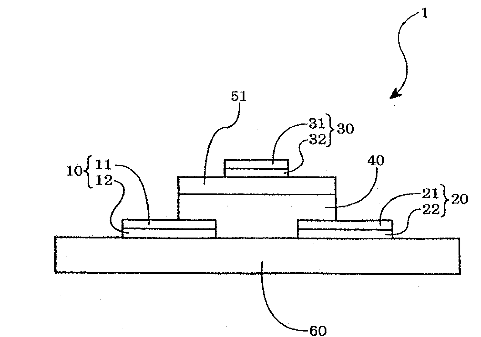
[0067]A first embodiment of a thin film transistor according to the present invention will be described.

[0068]FIG. 1 is an explanatory diagram showing outline of the first embodiment of the thin film transistor according to the invention.

[0069]In the example shown in the diagram, in a thin film transistor 1 as a field effect transistor, a drain electrode 10 and a source electrode 20 are formed so as to be apart from each other on a substrate 60, a transparent semiconductor thin film 40 is formed so as to be in contact with at least a part of each of the drain electrode 10 and the source electrode 20, and a gate insulating film 50 and a gate electrode 30 are formed in this order on the transparent semiconductor thin film 40. In such a manner, the thin film transistor 1 is constructed as the thin film transistor 1 of a top gate type.

[0070]In the embodiment, the materials of the gate electrode 30, the source electrode 20, and the drain electrode 10 are not particularly limited. Materia...

second embodiment

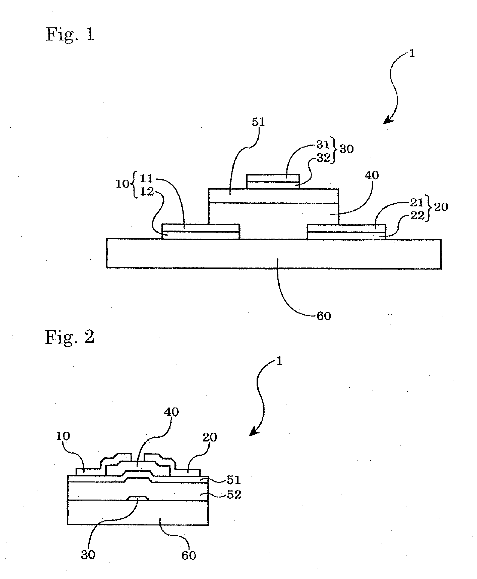
[0134]A second embodiment of the thin film transistor of the present invention will now be described.

[0135]FIG. 2 is an explanatory diagram showing outline of the second embodiment of the thin film transistor according to the present invention.

[0136]In the example of the diagram, in the thin film transistor 1, a gate insulating film B 52 and a gate insulating film A 51 are stacked in this order on the gate electrode 30 formed on the glass substrate 60 and, further, the transparent semiconductor thin film 40 is formed on the gate insulating film A 51. On both side parts of the transparent semiconductor thin film 40, the source electrode 20 and the drain electrode 10 are formed. In such a manner, the thin film transistor 1 of the bottom gate type is constructed.

[0137]In the foregoing first embodiment, the thin film transistor of the top gate type has been described. It can be a thin film transistor of the bottom gate type as in the second embodiment.

[0138]In the thin film transistor o...

third embodiment

[0140]A third embodiment of the thin film transistor of the present invention will now be described.

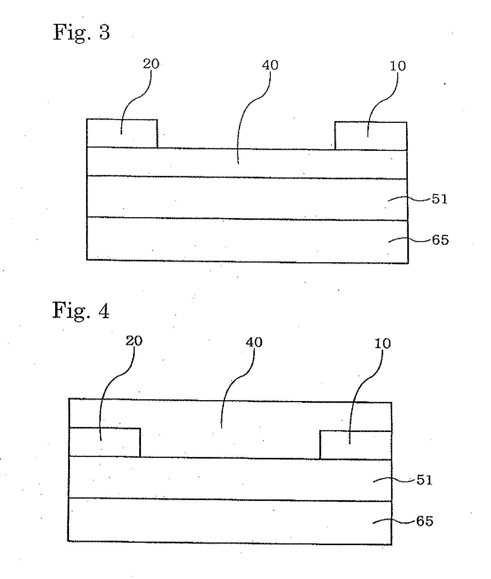
[0141]FIGS. 3 and 4 are explanatory diagrams showing outline of the third embodiment of the thin film transistor according to the present invention.

[0142]In the example shown in FIG. 3, in the thin film transistor 1, a gate insulating film 51 is stacked on a conductive silicon substrate 65 in which a gate electrode (not shown) is formed and, further, the transparent semiconductor thin film 40 is formed on the gate insulating film 51. On both side parts of the transparent semiconductor thin film 40, the source electrode 20 and the drain electrode 10 are formed. In such a manner, the thin film transistor 1 of the bottom gate type is constructed.

[0143]In the example shown in FIG. 4, in the thin film transistor 1, the gate insulating film 51 is stacked on the conductive silicon substrate 65 in which a gate electrode (not shown) is formed and, further, the source electrode 20 and the drain...


PUM

PropertyMeasurementUnit
Temperatureaaaaaaaaaa
Fractionaaaaaaaaaa

Abstract

A transparent semiconductor thin film 40 having low carrier concentration and a large energy band gap is produced by forming a thin film which contains indium oxide and an oxide of a positive divalent element, and then oxidizing or crystallizing the thin film.

Description

TECHNICAL FIELD[0001]The present invention relates to a semiconductor thin film containing indium, positive divalent element, and oxygen, a method for producing the same, and a thin film transistor using such a semiconductor thin film.BACKGROUND ART[0002]A field effect transistor is widely used as a unit electronic device of a semiconductor memory integrated circuit, a high-frequency signal amplification device, a liquid crystal drive device, or the like and is an electronic device which is most practically used at present.[0003]Among the devices, with remarkable development of displays in recent years, a thin film transistor (TFT) is often used as a switching device for driving a display by applying a drive voltage to a display device in not only a liquid crystal display (LCD) but also various displays such as an electroluminescence display (EL) and a field emission display (FED).[0004]As the material of the thin film transistor, a silicon semiconductor compound is used most widely...

Claims


Application Information

Patent Timeline
IPC IPC(8): H01L29/786H01L29/12C23C14/34H01L21/20
CPCC01G19/00C01P2006/40H01L29/66969H01L29/7869H01L29/66742H01L21/02554H01L21/02565H01L29/26
Inventor YANO, KOKIINOUE, KAZUYOSHISHIMANE, YUKIOSHIBUYA, TADAOYOSHINAKA, MASAHIRO
Owner IDEMITSU KOSAN CO LTD
Why Eureka
Try Eureka