This helps you quickly interpret patents by identifying the three key elements:
Problems solved by technology
Method used
Benefits of technology
Benefits of technology
[0030]Meanwhile, in case of an LSI using silicon, products manufactured by advanced micromachining, that is, 0.1 billion or more of metal-insulator-semiconductor field-effect transistor have already been integrated and mass produced. That is, since a device using the silicon may be easily installed on a high-quality single-crystal silicon substrate, a plurality of devices may be manufactured at a yield of approximately 100%. Therefore, even though a large amount of devices are integrated on the same chip, it is possible to economically increase the yield of the chip to a realistic level. Accordingly, an object of the present invention is to implement a light emitting device with high efficiency by using a IV-group semiconductor such as the silicon or germanium equivalent to the silicon.
[0035]In order to perform data communication between the chips or in the chip by using the light emitting device on a silicon substrate, not a simple LED but the light emitting device having strong directivity and monochromaticity is used, whereby an object of the present invention is to achieve a laser diode by oscillating the laser.
[0036]The present invention is made in view of the above-described objects. An object of the present invention is to provide a silicon laser device mainly constituted of silicon or a IV-group semiconductor such as germanium on a silicon substrate based on the silicon by a method capable of easily forming the silicon laser device with a general silicon process, and a method thereof.
[0038]A light emitting device according to an aspect of the present invention is an ultrathin silicon laser that includes a first electrode unit injecting electrons, a second electrode unit injecting holes, a light emitting unit electrically connected to the first electrode unit and the second electrode unit, wherein the light emitting unit is made of single-crystal silicon and has a first surface (top surface) and a second surface (bottom surface) opposed to the first surface, a waveguide made of a first dielectric, which is disposed in the vicinity of the light emitting unit, by setting surface directions of the first and second surfaces as a surface (100) and thinning a thickness of the light emitting unit in a direction perpendicular to the first and second surfaces, and a mirror formed by alternately adjoining the first dielectric and a second dielectric.
[0040]According to the present invention, it is possible to provide a silicon laser which can be easily formed on a substrate made of silicon, etc. by using a general silicon process at low price.
Problems solved by technology
A laser made of the compound semiconductor has very high efficiency, but it is expensive and is constituted of a plurality of elements, whereby it is difficult to control the laser.
Therefore, the laser is not integrated.
An OptoElectronic IC (hereinafter, referred to as ‘OEIC’) exists, but it is practically difficult to implement the OEIC by an optical device using the compound semiconductor.
However, the crystalline property worsens in the structure similar to the nanoparticle formed by a CVD (Chemical Vapor Deposition) method or a structure of which a surface has a plurality of irregular perforated holes by anode oxidation in comparison with a single crystal.
When the crystalline property worsens, the light is emitted at a defect level, but since it is inefficient in the light emission using a defect, it is impossible to manufacture a device capable of enduring a practical use such as the data communication, etc.
Method used
Image
Click on the blue label to locate the original text in one second.
Reading with bidirectional positioning of images and text.
Examples
first embodiment
[0131]In the embodiment, a silicon laser prepared by a method of easily forming the silicon laser by using a general silicon process and a manufacturing method thereof will be disclosed.
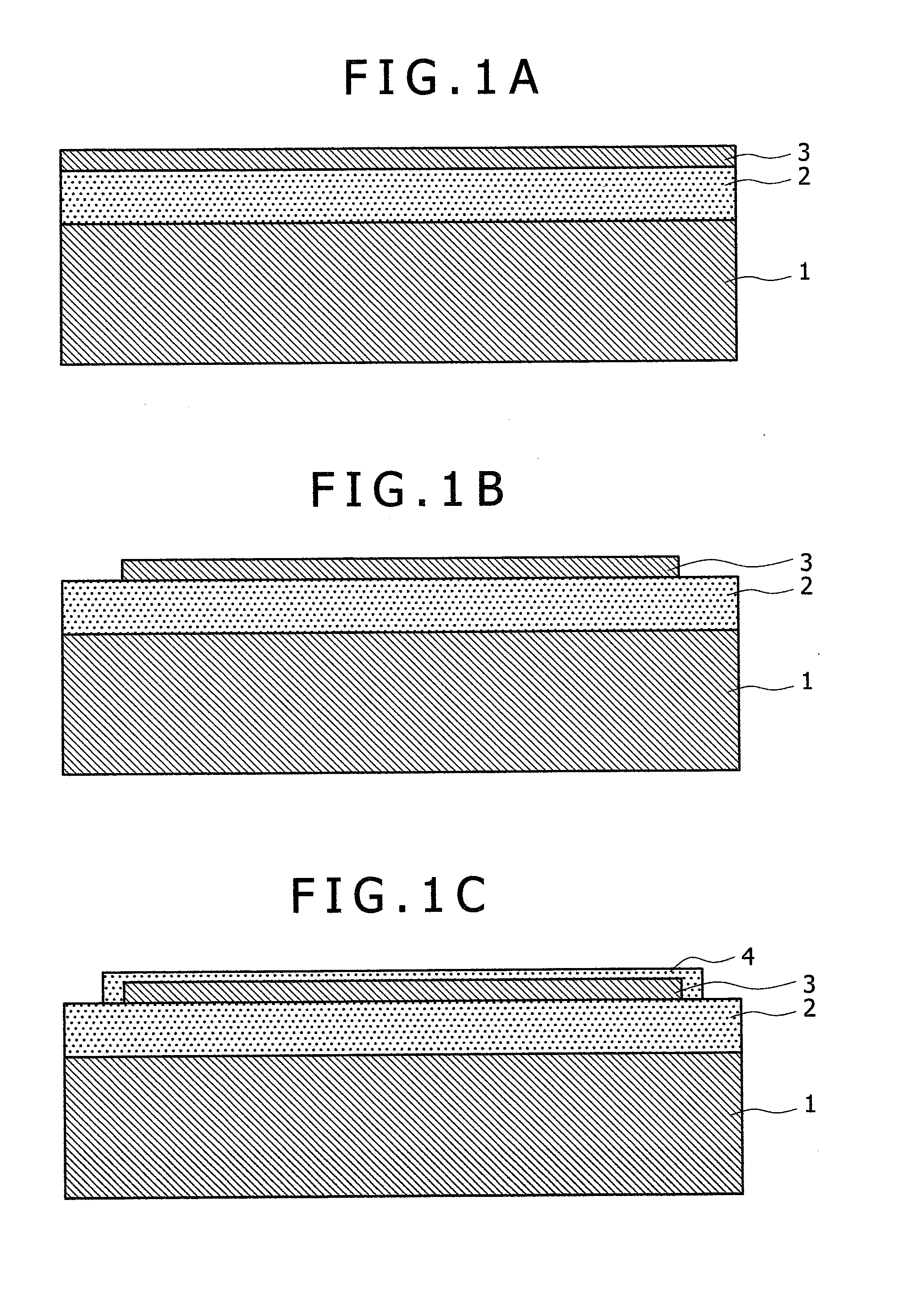
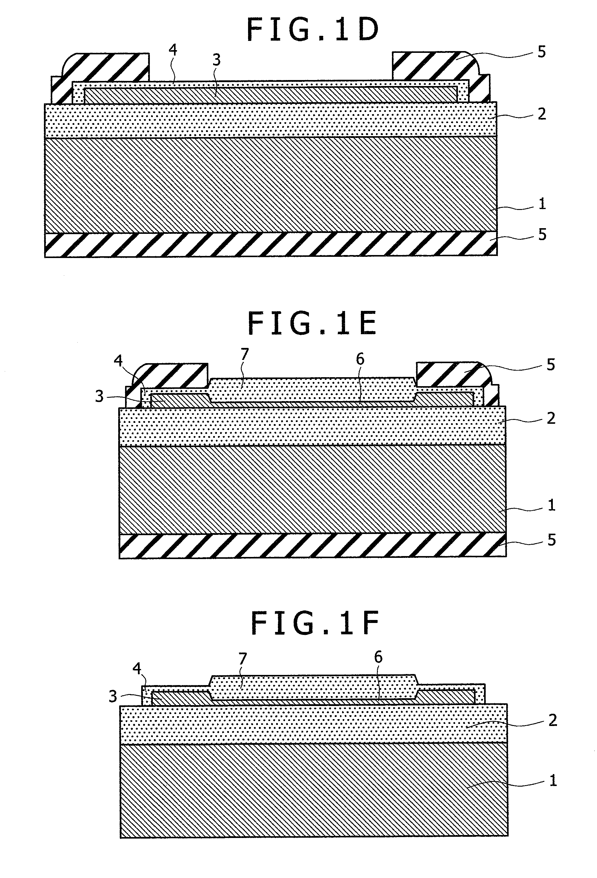
[0132]FIGS. 1A to 1R show cross-sectional structures of a manufacturing process sequence. FIGS. 2A to 2R are schematic views of a manufacturing process sequence viewed from an upper part of a substrate. Herein, FIGS. 1A to 1R are horizontal cross-sectional views of FIGS. 2A to 2R, respectively. For example, FIG. 1R shows a structure taken along a cross section 23 in FIG. 2R. In the embodiment, a completed drawing of a device is shown in FIGS. 1R and 2R.
[0133]Hereinafter, a manufacturing process will be sequentially described.
[0134]First, as shown in FIG. 1A, an SOI substrate as a support substrate is prepared on which a silicon substrate 1, a buried oxide (hereinafter, referred to as ‘BOX’) 2, and a silicon on insulator (hereinafter, referred to as ‘SOI’) 3 are laminated from the bottom thereof. Even...
second embodiment
[0165]In this embodiment, a silicon laser having a mirror structure and using a distributed Bragg reflector (hereinafter, referred to as ‘DBR’) and a manufacturing method thereof will be disclosed.
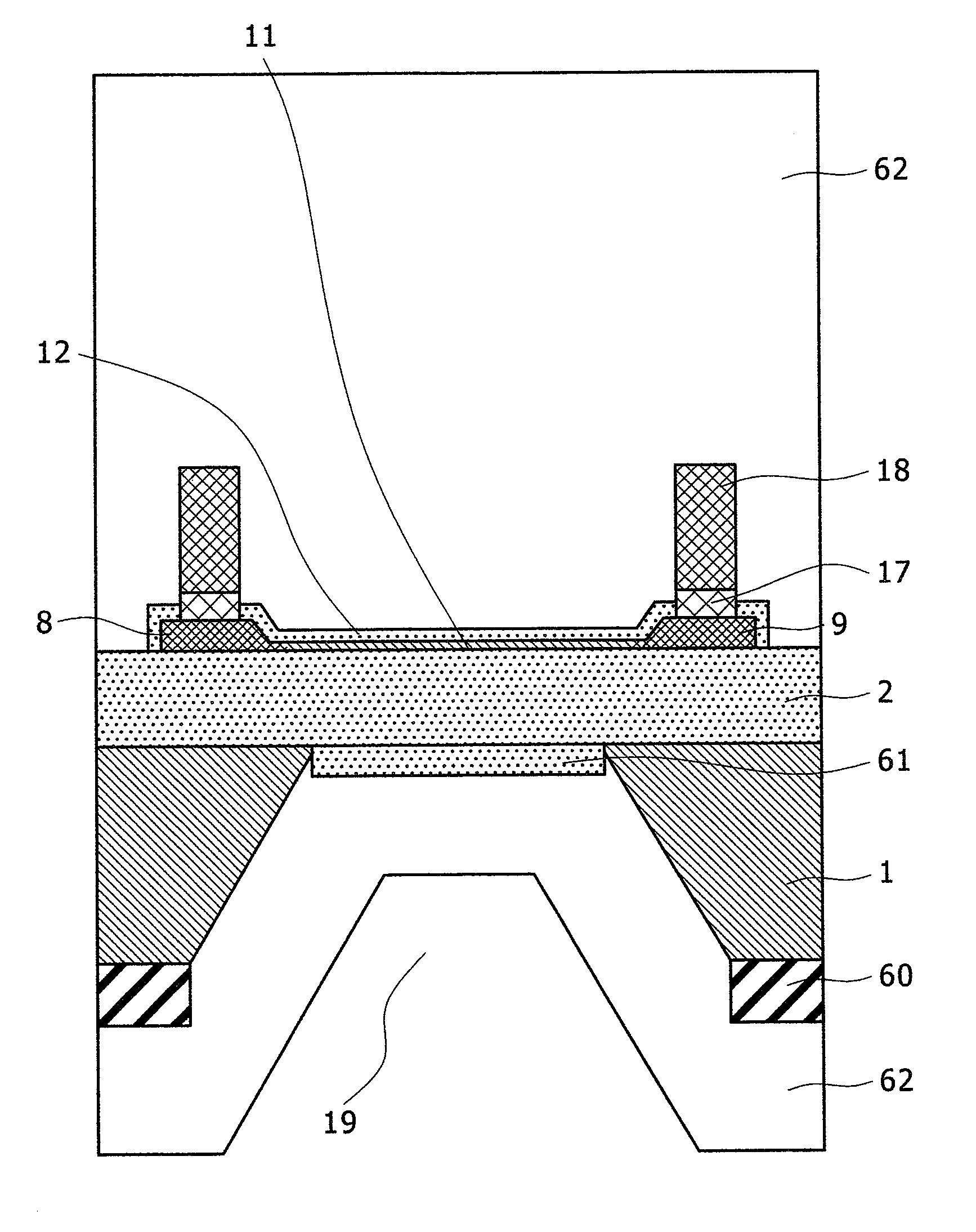
[0166]FIGS. 1A to 1G and FIGS. 3H to 3M show cross-sectional structures for each manufacturing process sequence. FIGS. 2A to 2G(2) and FIGS. 4H to 4M are schematic views of a manufacturing process from an upper part of a substrate. Herein, FIGS. 1A to 1G and FIGS. 3H to 3M are horizontal cross-sectional views of FIGS. 2A to 2G(2) and FIGS. 4H to 4M. For example, FIG. 3M shows a structure taken along a cross sectional 33 in FIG. 4M. In the embodiment, a completed drawing of a device is shown in FIGS. 3M and 4M.
[0167]First, after thin silicon 6 is formed by fabricating the device according to a manufacturing process sequence shown in FIGS. 1A and 1G and FIGS. 2A and 2G(2) by the same manufacturing process as the first embodiment, a p-type Si electrode 8 and an n-type Si electrode 9 are forme...
third embodiment
[0176]In this embodiment, a DFB type silicon laser and a manufacturing method thereof are disclosed.
[0177]FIGS. 1A to 1G and FIGS. 5H to 5K show a cross-sectional structure for each manufacturing process sequence. FIGS. 2A to 2G(2) and FIGS. 6H to 6K are schematic views of a manufacturing process from an upper part of a substrate. Herein, FIGS. 1A to 1G and FIGS. 5H to 5K are horizontal cross-sectional views of FIGS. 2A to 2G(2) and FIGS. 6H to 6K. For example, FIG. 5K shows a structure taken along a cross sectional 42 in FIG. 6H. In the embodiment, a completed drawing of a device is shown in FIGS. 3M and 4M.
[0178]First, after thin silicon 6 is formed by fabricating the device according to the manufacturing process sequence shown in FIGS. 1A and 1G and FIGS. 2A and 2G(2) by the same manufacturing process as the first embodiment, a p-type Si electrode 8 and an n-type Si electrode 9 are formed by injecting impurities and performing activation heat treatment thereon as shown in FIGS. 1...
PUM
Abstract
There are a siliconlaser device having a IV-group semiconductor such as silicon or germanium equivalent to the silicon as a basic constituent element on a substrate made of the silicon, and the like by a method capable of easily forming the silicon laser device by using a general silicon process, and a manufacturing method thereof. The silicon laser device is an ultrathin silicon laser that includes a first electrode unit injecting electrons, a second electrode unit injecting holes, a light emitting unit electrically connected to the first electrode unit and the second electrode unit, wherein the light emitting unit is made of single-crystal silicon and has a first surface (top surface) and a second surface (bottom surface) opposed to the first surface, a waveguide made of a first dielectric, which is disposed in the vicinity of the light emitting unit, by setting surface directions of the first and second surfaces as a surface (100) and thinning a thickness of the light emitting unit in a direction perpendicular to the first and second surfaces, and a mirror formed by alternately adjoining the first dielectric and a second dielectric.
Description
CLAIM OF PRIORITY[0001]The present application claims priority from Japanese patent application JP2007-262194 filed on Oct. 5, 2007, the content of which is hereby incorporated by reference into this application.BACKGROUND OF THE INVENTION[0002]1. Field of the Invention[0003]The present invention relates to a light emitting device using silicon, and more particularly, a laser using ultrathin silicon.[0004]2. Description of the Related Art[0005]An optical communication is adopted in a broadband network supporting an Internet industry. A laser using a compound semiconductor of the III-V group or II-VI group is used for transmission and reception using light in such an optical communication.[0006]Various structures are proposed for the compound semiconductor laser, but a double hetero structure is generally used. In the double hetero structure, a compound semiconductor having a small band gap is fitted in a compound semiconductor having a large band gap by using two different kinds of ...
Claims
Application Information
Patent Timeline
Application Date:The date an application was filed.
Publication Date:The date a patent or application was officially published.
First Publication Date:The earliest publication date of a patent with the same application number.
Issue Date:Publication date of the patent grant document.
PCT Entry Date:The Entry date of PCT National Phase.
Estimated Expiry Date:The statutory expiry date of a patent right according to the Patent Law, and it is the longest term of protection that the patent right can achieve without the termination of the patent right due to other reasons(Term extension factor has been taken into account ).
Invalid Date:Actual expiry date is based on effective date or publication date of legal transaction data of invalid patent.

