Apparatus and a method for inspection of a mask blank, a method for manufacturing a reflective exposure mask, a method for reflective exposure, and a method for manufacturing semiconductor integrated circuits

a mask blank and mask technology, applied in the field of apparatus and a mask blank inspection method, can solve the problems of inability to detect all defects causing phase change, inability to discriminate between concave and convex defects simultaneously, and inability to reduce the size of the mask blank, and achieve accurate and convenient inspection. , the effect of avoiding any defects

Active Publication Date: 2009-04-09
RENESAS ELECTRONICS CORP
View PDF9 Cites 91 Cited by
  • Summary
  • Abstract
  • Description
  • Claims
  • Application Information

AI Technical Summary

Benefits of technology

[0017]An object of the present invention is to provide an apparatus and a method for inspection of a mask blank, which can accurately and conveniently inspect presence / absence and types of defects in reflective mask blank.
[0018]Further, an object of the invention is to provide a method for manufacturing a reflective exposure mask, which can manufacture a reflective exposure mask with high reliability and yield even if presence of any defect has been proved by the above-described inspection method.
[0029]According to this embodiment, presence / absence and types of defects in a reflective mask blank can be accurately and conveniently inspected, thereby allowing factors of defect generation to be analyzed. Further, by utilizing the obtained defect positional information, the absorber pattern can be formed on the reflective mask blank so as to avoid any effects of defects, thereby improving the yield of the reflective exposure mask.

Problems solved by technology

In EUVL, because of reflective masks using Bragg reflection and an extreme short exposure wavelength of 13.5 nm, occurrence of even slight height irregularities as small as a fraction of the exposure wavelength may cause local differences in reflectivity due to those height irregularities, resulting in defects during transfer processes.
However, in JP-2003-114200 A, the dark field detection method employing EUV light is highly sensitive in detection and excellent in detection performance for phase defects due to irregularities of multilayer film, but incapable of discriminating between concave and convex defects simultaneously.
Also, in JP-6-349715 A (1994), the X-ray microscope method employing the bright field examines only the reflection ratio of the multilayer film, hence, all of defects causing changes in phase cannot be detected.
Also, in US 2004 / 0057107 A, the method, that is an exposure wavelength inspection serving as both a bright field inspection and a dark field inspection, involves more complicated inspection equipment and, although being a high-speed dark field inspection, yet is not highly sensitive in detection.
Also, as in JP-2001-174415 A, and JP-2002-333313 A, the method employing laser is insufficient in sensitivity because defects to be detected are too small as compared with the inspection wavelength.
Moreover, the method can detect concave and convex defects residing only on the surface of the multilayer film, but cannot capture defects which reside inside the multilayer film and may cause abnormalities of EUV light reflection.
Further, in JP-11-354404 A (1999), the method in which a peelable pattern is formed on the multilayer coated mask blank, and then actual pattern is transferred therewith, and then the pattern is examined to detect multilayer-film defects, can detect phase defects, but requires a further step of actual transfer of pattern transfer, resulting in cumbersome inspection.
In any of the inspection methods as described above, in case any defect that is hard to repair is detected, even if the defect is of minute size, the mask blank involved is regarded as a defective, being put into disposal.

Method used


Image

  • Apparatus and a method for inspection of a mask blank, a method for manufacturing a reflective exposure mask, a method for reflective exposure, and a method for manufacturing semiconductor integrated circuits
  • Apparatus and a method for inspection of a mask blank, a method for manufacturing a reflective exposure mask, a method for reflective exposure, and a method for manufacturing semiconductor integrated circuits
  • Apparatus and a method for inspection of a mask blank, a method for manufacturing a reflective exposure mask, a method for reflective exposure, and a method for manufacturing semiconductor integrated circuits

Examples


embodiment 1

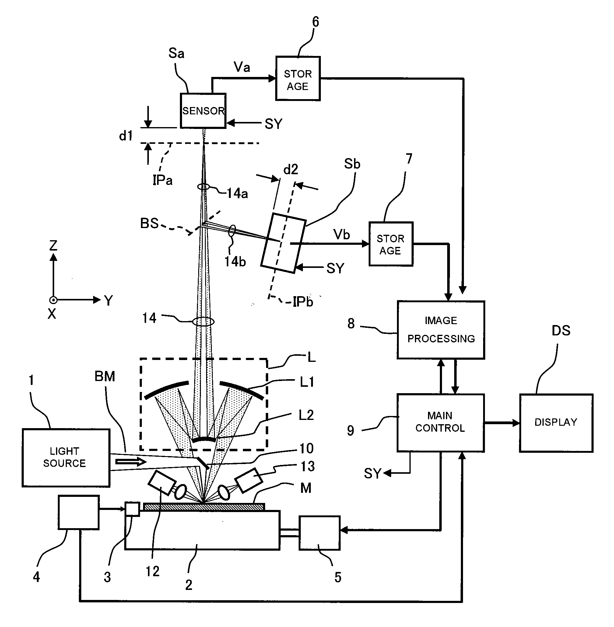
[0042]FIG. 1 is a configurative view showing an example of a mask blank inspection apparatus according to the present invention. The mask blank inspection apparatus is constituted of a stage 2 for mounting a reflective mask blank M thereon, a light source 1 for generating inspection light BM, a mirror 10 serving as an illuminating optics, an imaging optical system L, a beam splitter BS, two two-dimensional (2D) array sensors Sa and Sb, signal storage units 6 and 7, an image processing unit 8, a main control unit 9 for controlling operation of the whole apparatus. For easier understanding, it is assumed here that the stage surface is an XY plane and the direction normal to the stage surface is a Z axis.

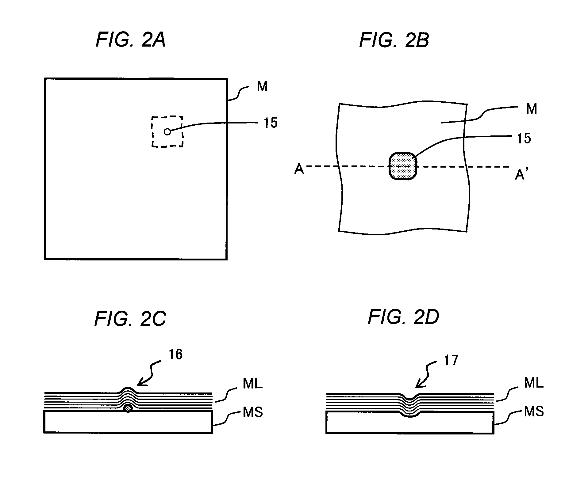
[0043]The mask blank M, as shown in FIG. 2, has a multilayer film ML on a mask substrate MS. The multilayer film ML is formed of Si (silicon) and Mo (molybdenum) alternately stacked to achieve a sufficient reflectance for exposure light of a wavelength (e.g., 13.5 nm). The mask substra...

embodiment 2

[0091]In this embodiment, exemplified here is a case where an optical branching element formed of a diffraction grating is used instead of the beam splitter BS in the inspection apparatus shown in FIG. 1.

[0092]FIG. 8A is a configurative view showing an example in which a transmissive diffraction grating GR1 is used. FIG. 8B is a configurative view showing an example in which a reflective diffraction grating GR2 is used. Components other than the optical branching element are similar to those of FIG. 1, and their redundant description is omitted.

[0093]In FIG. 8A, the diffraction grating GR1 is composed as a stencil transmissive diffraction grating, for example, with a group of linear openings having a pitch of 140 nm. As the light beam 14 outputted from the imaging optical system L passes through the diffraction grating GR1, the light beam may branch into several-order diffracted light according to a diffraction angle which can be determined by grating pitch and wavelength of light. ...

embodiment 3

[0099]In this embodiment, described below are a method for reflective exposure using the above-described reflective exposure mask, as well as a method for manufacturing semiconductor integrated circuits.

[0100]FIG. 9 is a configurative view showing an example of a reflective exposure apparatus. A mask M is manufactured according to the above-described mask manufacturing method. EUV light having a center wavelength of 13.5 nm emitted from a light source 40 illuminates a pattern surface of the mask M via an illumination optical system 41 composed of a plurality of multilayer-film reflecting mirrors. Light reflected from the pattern surface passes through a reduction-projection optics 42 (having a magnification of, e.g., ¼) composed of a plurality of multilayer-film reflecting mirrors to be focused onto a wafer 43. The wafer 43 is mounted on an in-plane movable stage 44. A pattern corresponding to the mask M is transferred to a desired region of the wafer 43 by repetition of movement of...


PUM

PropertyMeasurementUnit
wavelengthaaaaaaaaaa
wavelengthsaaaaaaaaaa

Abstract

The mask blank inspection apparatus is constituted of a stage for mounting a reflective mask blank thereon, a light source for generating inspection light, a mirror serving as an illuminating optics, an imaging optical system, a beam splitter, two two-dimensional array sensors, signal storage units, an image processing unit, a main control unit for controlling operation of the whole apparatus, the first sensor being located at a position which is displaced by a predetermined distance from the focal plane of a first light beam, the second sensor being located at a position which is displaced by a predetermined distance from the focal plane of a second light beam along a opposite direction, whereby accurately and conveniently inspecting presence / absence and types of defects in reflective mask blank.

Description

BACKGROUND OF THE INVENTION[0001]1. Field of the Invention[0002]The present invention relates to an apparatus and a method for inspection of a mask blank suitable for, for example, EUVL (Extreme Ultra Violet Lithography) using extreme ultraviolet radiation with a wavelength of about 13.5 nm. The invention also relates to a method for manufacturing a reflective exposure mask, a method for reflective exposure, as well as a method for manufacturing semiconductor integrated circuits.[0003]2. Description of the Related Art[0004]Semiconductor devices, such as semiconductor integrated circuits, are mass produced by repetitively using a optical lithography process in which a mask, i.e., a master having a circuit pattern drawn thereon, is irradiated with exposure light so that the pattern is transferred onto a semiconductor substrate (hereinafter, referred to as “wafer”) via reduction projection optics.[0005]In recent years, as scale-down of semiconductor devices have been progressing, there...

Claims


Application Information

Patent Timeline
Patent Type & Authority Applications(United States)
IPC IPC(8): G01N21/956G01N21/88G03F1/22G03F1/24H01L21/027
CPCG01N21/47G01N21/956G03F1/84G01N2021/95676G01N2021/4711
Inventor TERASAWA, TSUNEOTANAKA, TOSHIHIKOAOTA, TATSUYA
Owner RENESAS ELECTRONICS CORP
Why Eureka
Try Eureka