Semiconductor device and manufacturing method thereof

a semiconductor device and manufacturing method technology, applied in the direction of semiconductor devices, bulk negative resistance effect devices, electrical appliances, etc., can solve the problems of difficult to form thin metal films having a thickness less than 10 nm, difficult to control the thickness of metal silicide layers, and low yield of transistors, so as to improve the subthreshold swing and improve the operation speed of semiconductor devices. , the effect of high yield

Inactive Publication Date: 2009-04-16
SEMICON ENERGY LAB CO LTD
View PDF10 Cites 213 Cited by
  • Summary
  • Abstract
  • Description
  • Claims
  • Application Information

AI Technical Summary

Benefits of technology

[0010]A first object of the present invention is to provide a thin film transistor (a semiconductor device) in which a metal silicide layer is formed on a surface of a doped region and entrance of the metal silicide into a channel formation region is surely prevented, and which generates less heat, consumes less power, and can be manufactured in a high yield; and a method for manufacturing the thin film transistor.
[0011]A second object of the present invention is to provide a thin film transistor (a semiconductor device) in which a metal silicide layer is formed on a surface of a doped region and entrance of the metal silicide into a channel formation region is surely prevented, and which generates less heat, consumes less power, can be manufactured in a high yield, and in which the thickness of a channel formation region is smaller than that of a source region and a drain region, and subthreshold swing is improved; and a method for manufacturing the thin film transistor.

Problems solved by technology

In such a transistor having a metal silicide layer, however, the metal silicide can undesirably enter a channel formation region to cause a malfunction of the transistor.
In particular, when a semiconductor film is thin, it is difficult to control the thickness of the metal silicide layer.
In forming a metal silicide layer, the thermal treatment temperature, the thermal treatment time, and the thickness of the metal film are controlled; however, since it is difficult to control the thermal treatment, a method can be given in which the entire metal film which has been formed with the thickness controlled reacts with silicon in the semiconductor film.
In such a method, when the semiconductor film is thin, the metal film also needs to be thinned (e.g., to a thickness of less than 10 nm) accordingly; however, it is difficult to form a thin metal film having a thickness of less than 10 nm, with the thickness controlled in nanometers.
However, such a change of the part of the source / drain region to amorphous silicon complicates a process and increases manufacturing cost.
By forming the thin oxide film on the surface of the n+-Si film in such a manner, the thickness of the metal silicide layer formed between the n+-Si film and the metal film can be minimized, which facilitates etching of the metal silicide layer In such a manufacturing method of a thin film transistor, however, the gate electrode needs to withstand a high temperature or the like in forming the semiconductor film because the source and drain regions (the semiconductor film) are formed over the gate electrode after forming the gate electrode; therefore, there are limitations on the material or thickness of the gate electrode.
In particular, when a polycrystalline silicon film is formed as the semiconductor film, a method can be given in which an amorphous silicon film is annealed with laser to form polycrystalline silicon; however; in a bottom gate structure, it is difficult to carry out laser annealing because of limitations such as heat resistance or thermal conductivity of the gate electrode.
Further, a bottom gate structure cannot be formed on an SOI (silicon on insulator) substrate in which a single crystalline silicon layer is formed on an insulator using an SOI technique such as the Smart Cut method.
However, when an entire semiconductor film in which a channel formation region is formed is thinned in order to thin the channel formation region, a source region and a drain region are also thinned; thus, there arise problems of increase in sheet resistance in the source and drain regions and increase in contact resistance between the source and drain regions and source and drain electrodes.

Method used


Image

  • Semiconductor device and manufacturing method thereof
  • Semiconductor device and manufacturing method thereof
  • Semiconductor device and manufacturing method thereof

Examples


Embodiment Construction

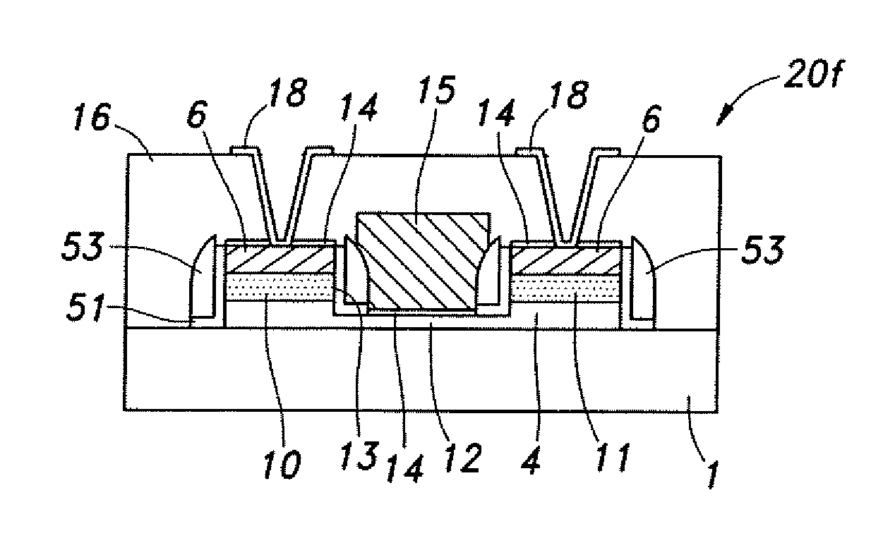
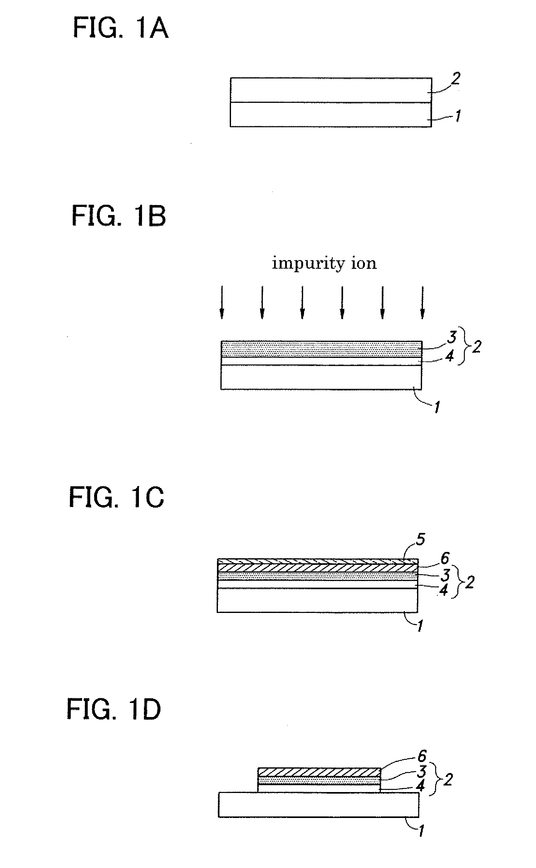
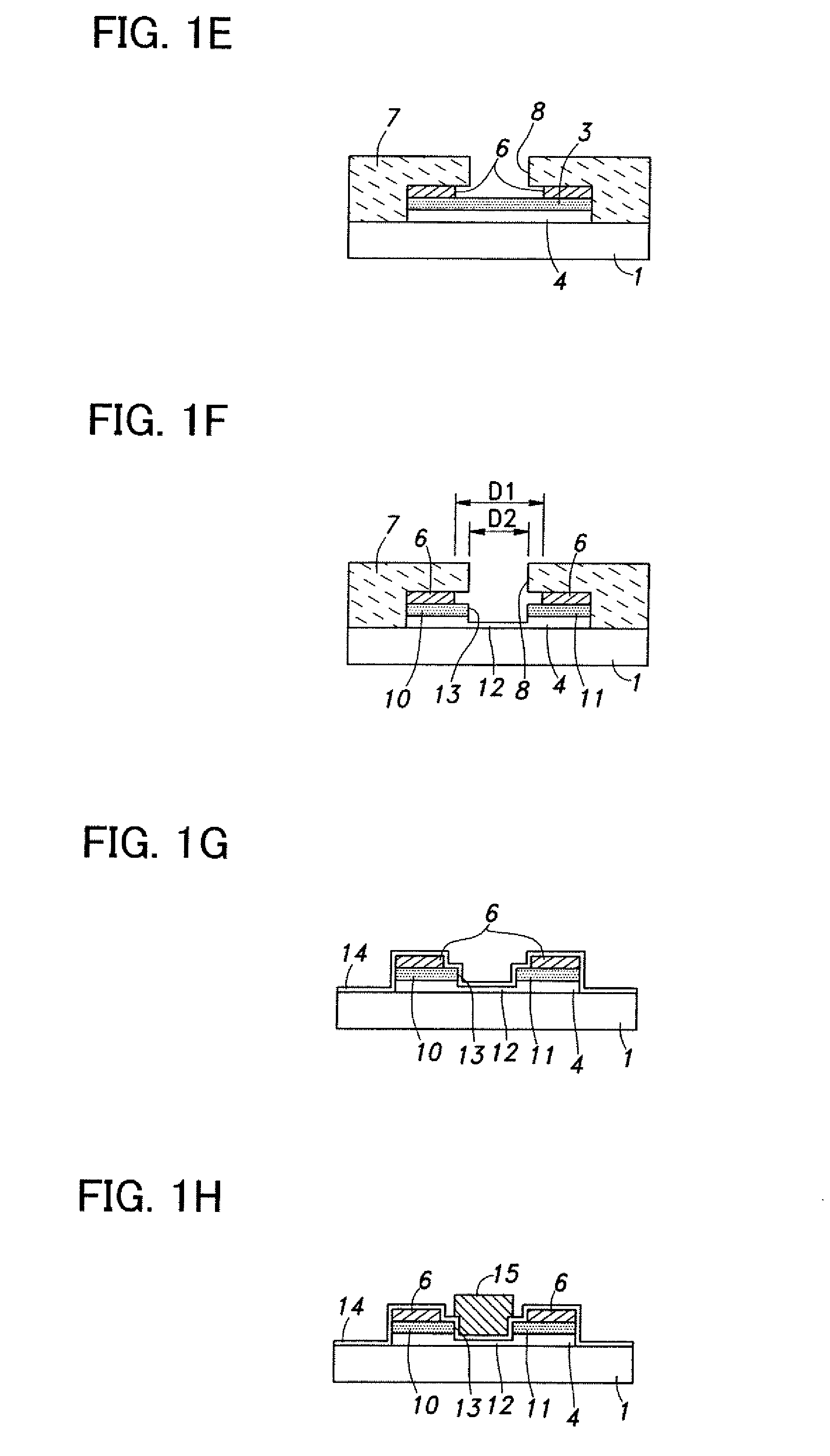
[0039]FIGS. 1A to 1J are cross-sectional views showing a method for manufacturing a semiconductor device (TFT) based on a preferred embodiment of the present invention.

[0040]First, as shown in FIG. 1A, a semiconductor film 2 is formed over an insulating substrate 1, using a semiconductor material including silicon. As the insulating substrate 1, a glass substrate, a quartz substrate, a heat-resistant plastic substrate, or the like can be used. If a glass substrate is used, it is preferable that a base film be formed on a surface of the glass substrate in order to prevent impurity ions (e.g., of Na) from the glass substrate from entering the semiconductor film 2. Further, as the insulating substrate 1, it is also possible to use a single crystalline silicon substrate or a metal substrate whose surface is provided with an insulating base film. Such a base film is only required to be formed of an insulating material having a heat-resistant property and a chemical-resistant property whi...


PUM

PropertyMeasurementUnit
thicknessaaaaaaaaaa
thicknessaaaaaaaaaa
thicknessaaaaaaaaaa

Abstract

In a method for manufacturing a semiconductor device, a semiconductor film formed over an insulator is doped with an impurity element to a depth less than the thickness of the semiconductor film, thereby forming an impurity doped layer; a metal silicide layer is formed on the impurity doped layer; the metal silicide layer and the semiconductor film are etched to form a recessed portion; and a layer which is not doped with the impurity element and is located at the bottom of the recessed portion of the semiconductor film is thinned to make a channel formation region. Further, a gate electrode is formed in the recessed portion over the thinned non impurity doped layer, with an insulating film interposed therebetween.

Description

BACKGROUND OF THE INVENTION[0001]1. Field of the Invention[0002]The present invention relates to a semiconductor device and a manufacturing method thereof; in particular, to a semiconductor device having metal silicide layers on a source region and a drain region, and a manufacturing method thereof.[0003]2. Description of the Related Art[0004]As higher integration and further miniaturization of a semiconductor device such as a thin film transistor (also referred to as a TFT) are achieved, lower contact resistance with a doped region (e.g., a source region or a drain region of a transistor) formed in a semiconductor film including silicon, and lower resistance of the doped region have been required. It is effective in lowering the resistance to form a metal silicide layer such as a titanium silicide layer, a cobalt silicide layer, or a nickel silicide layer on a surface of the semiconductor film. Reduction in the resistance of the doped region and in the contact resistance therewith ...

Claims


Application Information

Patent Timeline
Patent Type & Authority Applications(United States)
IPC IPC(8): H01L47/00H01L21/20
CPCH01L29/458H01L29/66757H01L29/66621
Inventor SHINGU, TAKASHIOHGARANE, DAISUKESATO, YURIKA
Owner SEMICON ENERGY LAB CO LTD
Why Eureka
Try Eureka