Low-cost multi-junction solar cells and methods for their production

Active Publication Date: 2009-05-14
SUNPREME
View PDF64 Cites 27 Cited by
  • Summary
  • Abstract
  • Description
  • Claims
  • Application Information

AI Technical Summary

Benefits of technology

[0028]Features of the invention enable achieving a production-worthy solution to the abovementioned problems, by, among others, fabricating a solar cell structure that capitalizes on the conversion efficiency of bulk silicon wafers and the benefits of thin film cell structures. According to aspects of the invention, the solar cell is fabricated by utilizing silicon wafers made of very low cost metallurgical-grade silicon as the substrate, and fabricating a thin-film solar cell on the substrate. According to features of the invention, the cells are fabricated by depositing thin films of very small th

Problems solved by technology

Conventional energy generation from fossil fuels represents the greatest threat since the last ice age to the planet's well being.
However, despite over thirty years of work, silicon-based solar cells have not performed up to their potential for large-scale power generation.
A major barrier to such acceptance is the cost associated with fabricating solar cells, and especially the cost of raw, base material (substrates) used to fabricate the solar cells.
Ironically, because of enormous demand and high production costs, the price of the silicon material for solar cells actually increases in tandem with the price of oil.
For example, over the past few years the cost per kg of polysilicon material used to produce solar silicon wafers has increased dramatically, and for thin-film solar cells the cost of Silane gas used to deposit the film as well as that of NF3 gas to clean up the reactors following deposition have similarly increased.
First, large quantities of silicon wafers are produced for the substrate—typically a million wafers per month for a rather modest 25 MW capacity factory.
These gases are both highly flammable and toxic.
However, due to the environmental and health hazards in the gasification of silicon, few factories operate in the world, thereby causing a bottleneck for the semiconductor and solar cell industry.
Newly proposed silicon gasification factories face resistance from local communities based on environmental and safety concerns.
These factories also require large capital investments and long lead times. Consequently, there is always an imbalance between demand and supply of bare silicon wafers.
That is, in commercial terms, the process of transforming a silico

Method used


Image

  • Low-cost multi-junction solar cells and methods for their production
  • Low-cost multi-junction solar cells and methods for their production
  • Low-cost multi-junction solar cells and methods for their production

Examples


example i

[0062]Metallurgical grade silicon of three nines was produced by inductively melting silicon pellets of two nines in a graphite crucible of about 1.5 m×1.5 m, and then slowly cooling into a cylindrical shape over 24 hrs. The carbon-rich surface crust was removed, and the cylinder crushed into grains or pellets. The resulting material contained both B and P, but was generally p-type with resistivity in the range 0.1-1 ohmcm. The resulting material was then cast into metallurgical grade silicon ingot of about 0.5 m×1 m, with controlled cooling and dopant adjustment. Metallurgical grade silicon wafers were fabricated by machining 6 in. cores out from the ingot, the cylinder surface was smoothed and then 500 μm thick wafers were sawed off the cylinders. One surface was mechanically polished, and both surfaces were lightly etched to reveal the large polygonal grain structure on the back of the wafer. This resulted in about 500 metallurgical grade silicon wafers of four nines and five nin...

example ii

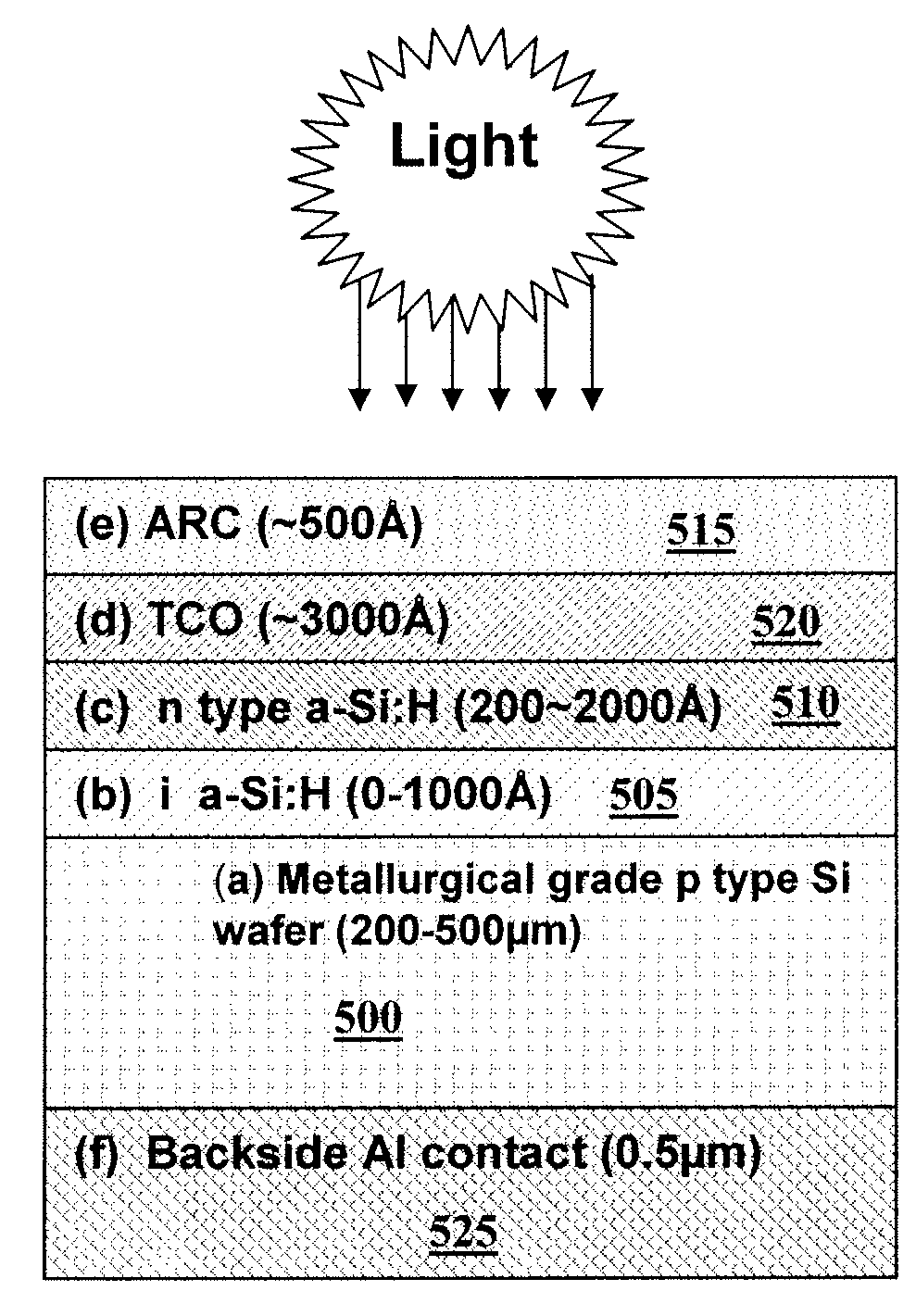
[0064]A single hetrojunction with an intrinsic passivation layer device structure is formed on low-cost metallurgical-grade substrates by depositing a nano-scale Si:H film stack on the front, i.e., “device” side, and an oppositely doped a-Si:H film on the back “contact” side. The metallurgical-grade substrates obviates the need and expense of aggressively thinning the substrate from 500 to 250 μm as is done for crystalline Si substrates. The thicker wafers provide more robust handling in automated process lines. This material also avoids the cost, cycle time and complexity of polysilicon based gasification, solidification, melt-and-pull process, since the active device is created by a thin Si:H film just outside of the metallurgical-grade substrates surface that is passivated by a nano-scale intrinsic a-Si:H film.

[0065]The metallurgical-grade substrates may be formed in standard, e.g., 6-in, 8-in, 12-in, sizes, which can be processed in standard semiconductor PECVD processing equipm...

example iii

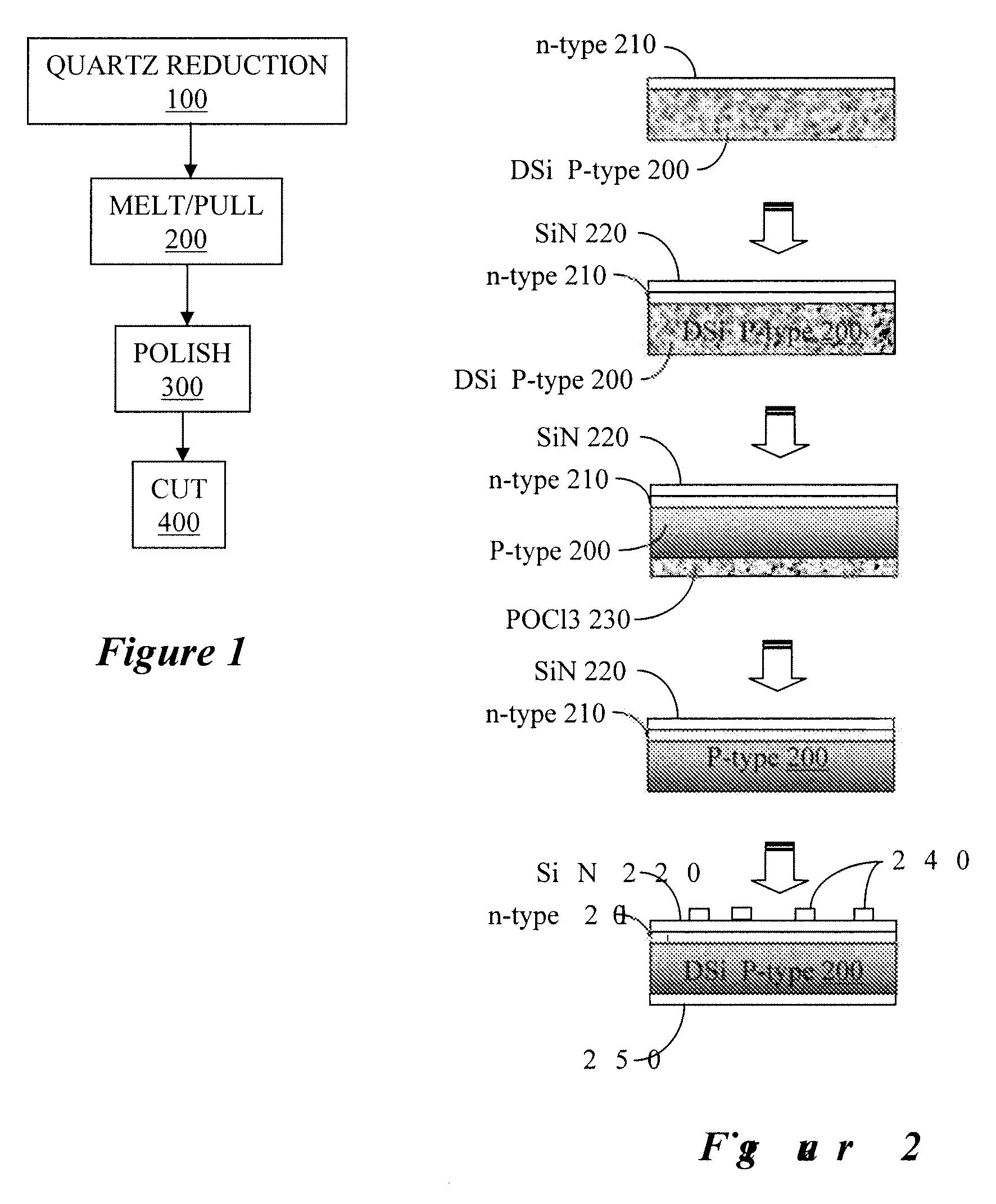
[0066]FIG. 9A illustrates an example of a process for fabricating a solar-cell ready substrate, generally referred to herein as SmartSi™. In step 900 metallurgical grade quartz is melted and reduced in an electrolytic cell containing graphite electrode and is then let cool and solidify to provide a ingot of about two nines metallurgical silicon. The ingot is broken into pellets, treated in chemicals to leach surface impurities and then cast into ingot. The ingot is then striped of its crust and broken into nuggets of three to four nines metallurgical silicon. The resulting nuggets are sorted according to their resistivity.

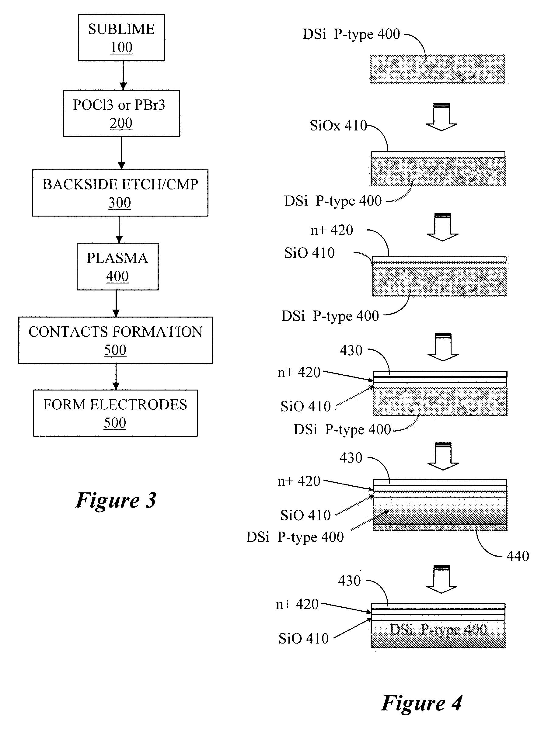
[0067]The sorted nuggets of MG silicon are cast in step 915. The melt is allowed to solidify into an ingot, which in step 920 is machined, cut into wafers, and the wafers are polished. In step 925 a PECVD chamber is used to form a thin layer of intrinsic amorphous silicon, i-a-Si:H, to passivate the surface of the MG-Si substrate. In step 930 a PECVD chamber is use...


PUM


Abstract

Methods for fabricating solar cells without the need to perform gasification of metallurgical-grade silicon are disclosed. Consequently, the costs and health and environmental hazards involved in fabricating the solar or silicon grade silicon are being avoided. A solar cell structure comprises a metallurgical grade doped silicon substrate and a thin-film structure formed over the substrate to form a p-i-n junction with the substrate. The substrate may be doped p-type and the thin film structure may be an intrinsic.

Description

RELATED APPLICATIONS[0001]This application claims priority benefit from U.S. Provisional Application Ser. No. 60 / 986,996, Filed on Nov. 9, 2007, the disclosure of which is incorporated herein in its entirety.BACKGROUND[0002]1. Field of the Invention[0003]The subject invention relates to solar photovoltaic cells and, more specifically, to method for manufacturing low cost base material for such cells and method for manufacturing low cost cells and the resulting cell device structure.[0004]2. Related Art[0005]Conventional energy generation from fossil fuels represents the greatest threat since the last ice age to the planet's well being. Among all of the alternative energy sources, next to conservation, solar photovoltaic cells are arguably the cleanest, ubiquitous and potentially most reliable alternative compared to other approaches such as ethanol, hydropower and wind power. The concept is a simple solid-state p-n junction that converts light into a small dc voltage. The cells may ...

Claims


Application Information

Patent Timeline
IPC IPC(8): H01L31/00
CPCH01L31/0256H01L31/04Y02E10/547H01L31/1804H01L31/0747Y02E10/548Y02P70/50
Inventor SINHA, ASHOK
Owner SUNPREME
Why Eureka
Try Eureka