[0008]Accordingly, the present invention is directed to a programmable memory built-in self-test circuit to meet the
test requirements in various applications, advance the
test quality in
mass production, compact the circuit, reduce the chip area and support memory complier and built-in self-repair function (BISR function).
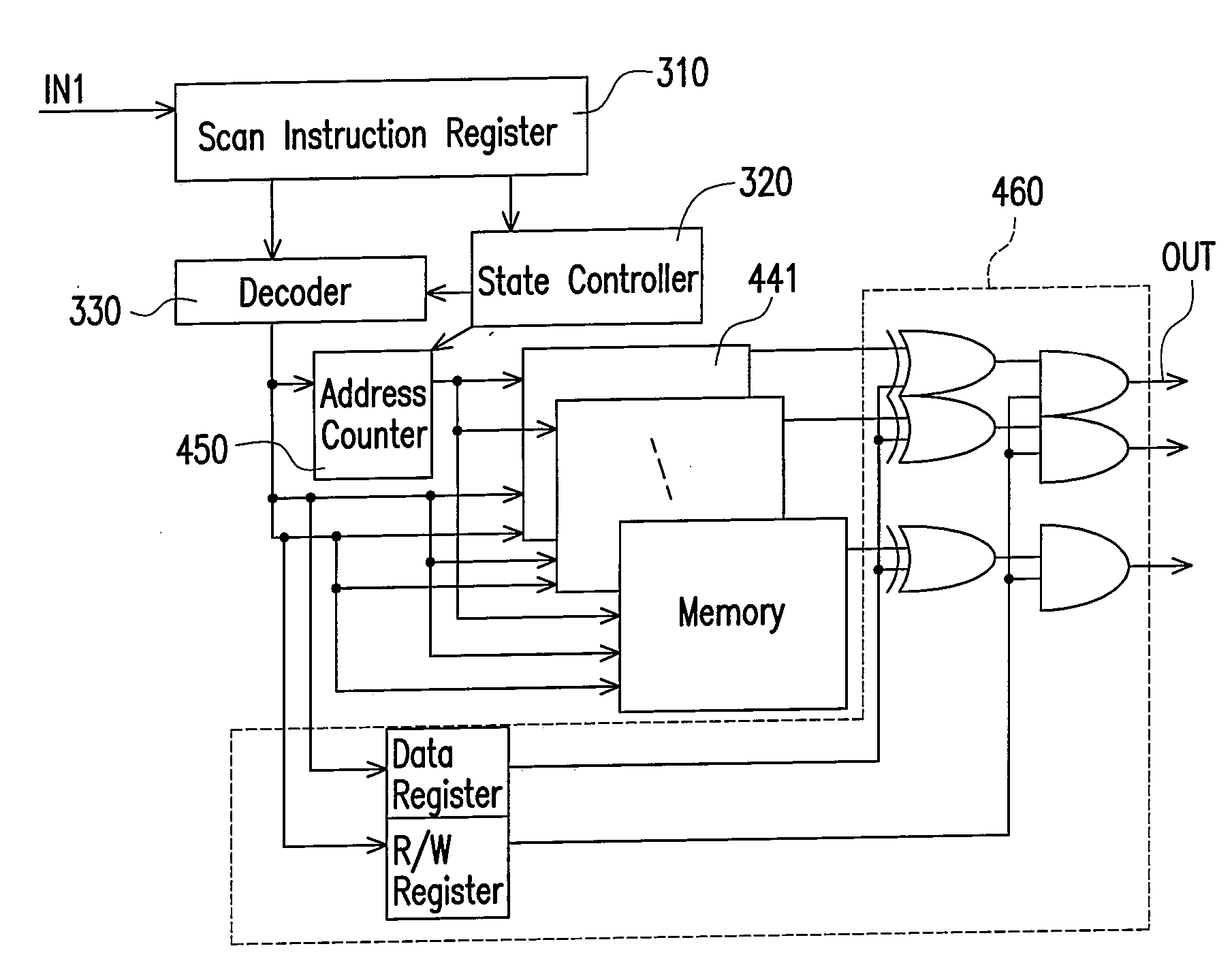
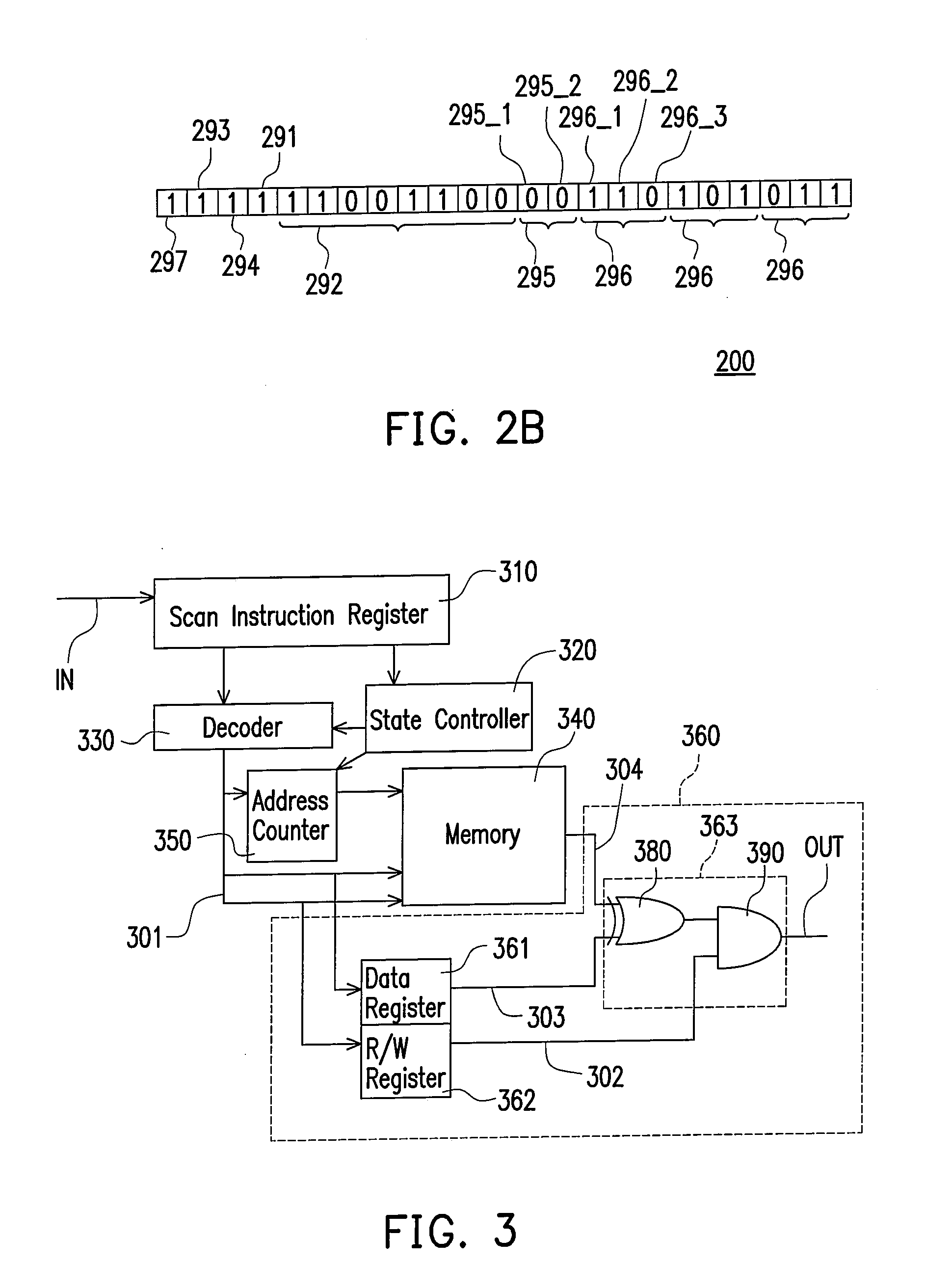
[0009]The present invention provides a memory built-in self-test circuit (MBIST circuit), which includes an
instruction decoder and a built-in self-test controller (BIST controller). The
instruction decoder is coupled with the BIST controller for receiving a
control signal, while the BIST controller is for receiving the
control signal. If the
control signal is in a self-test mode, the instruction decoder
decodes a self-test instruction, and the BIST controller tests the memory according to the decoded result of the self-test instruction. If the control
signal is in an output mode, the instruction decoder suspends its operation, and the BIST controller outputs the test
record of the memory. If the control
signal is in a
normal mode, the instruction decoder suspends its operation, and the BIST controller delivers the test
signal of a functional circuit to the memory. In this way, a user is able to flexibly conducts switching between the
normal mode and the self-test mode, observe the output status, easily conduct diagnosis and shorten
time schedule to lunch a product on market.
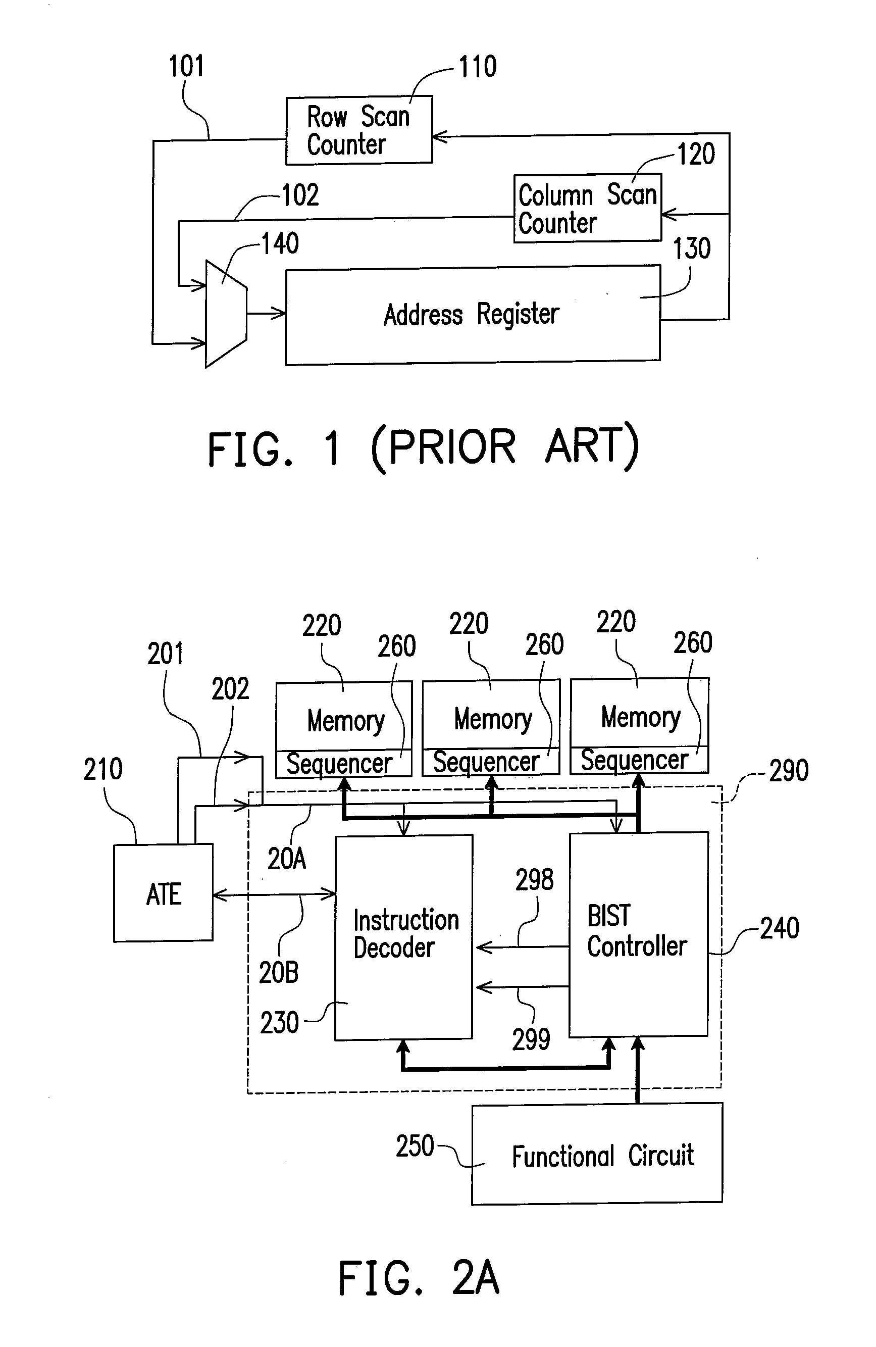
[0011]A conventional programmable MBIST circuit usually requires a scan register, an
instruction register and a
control register, wherein when a self-test instruction is output from a test
machine to a chip-under-test (
CUT), the instruction is received by the scan register, and then sent to the
instruction register for storage. Thereafter, the instruction is sent out for circuit operations, following by sending appropriate operation results, such as data, address, memory enabling (CE) and reading / writing enabling (WE), to the
control register for controlling the operations of the memory. The present invention further provides register sharing capability. With the register sharing capability, as long as the control signal of the memory can be generated directly by the
instruction register, the instruction register is competent to accomplish the above-mentioned three tasks, which facilitates reducing the chip area.
[0012]The present invention provides an address counter, which includes a address register, a rising-transition scrambler, a row scan
adder and a falling-transition scrambler, wherein the address register is for storing and providing the access address of a memory, the rising-transition scrambler is coupled with the address register and receives the access address from the address register, the row scan
adder is coupled with the rising-transition scrambler for adding a binary ‘1’ to the address output from the rising-transition scrambler and then outputting the above-mentioned address, and the falling-transition scrambler is coupled with the row scan
adder for receiving the address output from the row scan adder. If a memory has 2n addresses in total and each column has 2n addresses, the address of the memory has n bits and r folded bits, wherein n and r are preset integers. Based on the design principle of the present invention, if it is a row scan, the value of the address register is directly sent to the row scan adder, after adding a binary ‘1’ thereto, an updated address is obtained, that is, an operation of moving the address of a row scan is accomplished. If it is a column scan, the rising-transition scrambler moves the lower r bits to the highest bit position, right-shifts the higher (n-r) bits by r bits and then sends the address to the row scan adder for adding ‘1’ thereto. Thereafter, the falling-transition scrambler moves the higher r bits to the lowest bit position, left-shifts the lower (n-r) bits by r bits so as to generate an updated address. In this way, an operation of moving the address of a column scan is accomplished.
[0013]The present invention provides a clock switching circuit, wherein two enabling signals are used to control two clock signals, and negative edge-triggered
delay flip-
flops are used to control the enabling signals to avoid unexpected ‘0’ or ‘1’ clock
hazard. The approach is able to directly conduct a design of
register transfer level (RTL). Once paying attention that one of the above-mentioned clock enabling signals is turned off firstly, following by turning on another clock enabling signal, the synthesis and the placing and routing transistors are very easily conducted where there is no worry about any timing problem caused by a process drift or a logic operation speed; as a result, the clock switching is very stable.
[0014]Since the present invention adopts a lot of novel ideas to compact the chip area of a programmable MBIST circuit, a lower production cost is achieved. The present invention supports more functions with more flexibilities of self-testing a memory. In addition, the present invention also provides a
peripheral control circuit for increasing the test
fault coverage with a less chip area. In particular, the clock switching circuit of the present invention enables correct switching of the test clock between the MBIST circuit and the external test
machine, which makes the memory test and diagnosis more flexible.

