Method for producing organic electronic devices on solvent-and/or temperature-sensitive plastic substrates

a technology of temperature-sensitive plastics and electronic devices, which is applied in the direction of discharge tube luminescnet screens, sustainable manufacturing/processing, and final product manufacturing, etc., can solve the problems of inability to protect abs-substrates, polycarbonate substrates or polystyrene substrates from the damaging effects of solvents during the manufacturing process, and the application of polysiloxane layers is not possible to protect abs-substrates, polycarbonate substrates or

Inactive Publication Date: 2009-05-21
THURINGISCHES INSTITUT FUR TEXTIL & KUNST FORSCHUNG
View PDF2 Cites 12 Cited by
  • Summary
  • Abstract
  • Description
  • Claims
  • Application Information

AI Technical Summary

Benefits of technology

[0008]It is an object of the present invention to provide a simple and low-priced method for producing organic field-effect transistors (OFETs), solar cells or light emitting diodes (OLEDs) on the surface of solvent- and temperature-sensitive plastics, which permits to manufacture such semiconductor components and circuits based thereon without any deterioration of the molded body such as an incipient dissolving of the surface or thermal deformation of the same.

Problems solved by technology

They have, however, the disadvantage, compared to organic protective layers that they have to be precipitated by expensive and time-consuming vacuum processes.
WO 2004 / 091001 discloses a gate insulator for an organic semiconductor component, in particular for a field-effect transistor, which consists of a polysiloxane compound crosslinked at temperatures between 150° C. and 200° C. However, owing to the high crosslinking temperature, an application of the polysiloxane layer is not possible for protecting the ABS-substrates, polycarbonate substrates or the polystyrene substrates against the damaging effects of the solvents during the manufacturing procedure, apart from the fact that the polysiloxane layer is here used for electrical insulation.
But obviously it does not serve to protect the substrate against chemical actions by solvents.
In addition, mostly their thermal load capacity is only low.
Furthermore, the roughness of the surface of the employed injection molding tool also determines the surface roughness of the substrate so that the injection molded materials as basis materials for organic electronics are suited only strongly limited.
Due to the above mentioned reasons the use of these materials was heretofore problematic and there was not any suitable solution to overcome the difficulties mentioned hereinbefore.

Method used


Image

  • Method for producing organic electronic devices on solvent-and/or temperature-sensitive plastic substrates
  • Method for producing organic electronic devices on solvent-and/or temperature-sensitive plastic substrates
  • Method for producing organic electronic devices on solvent-and/or temperature-sensitive plastic substrates

Examples


example 2

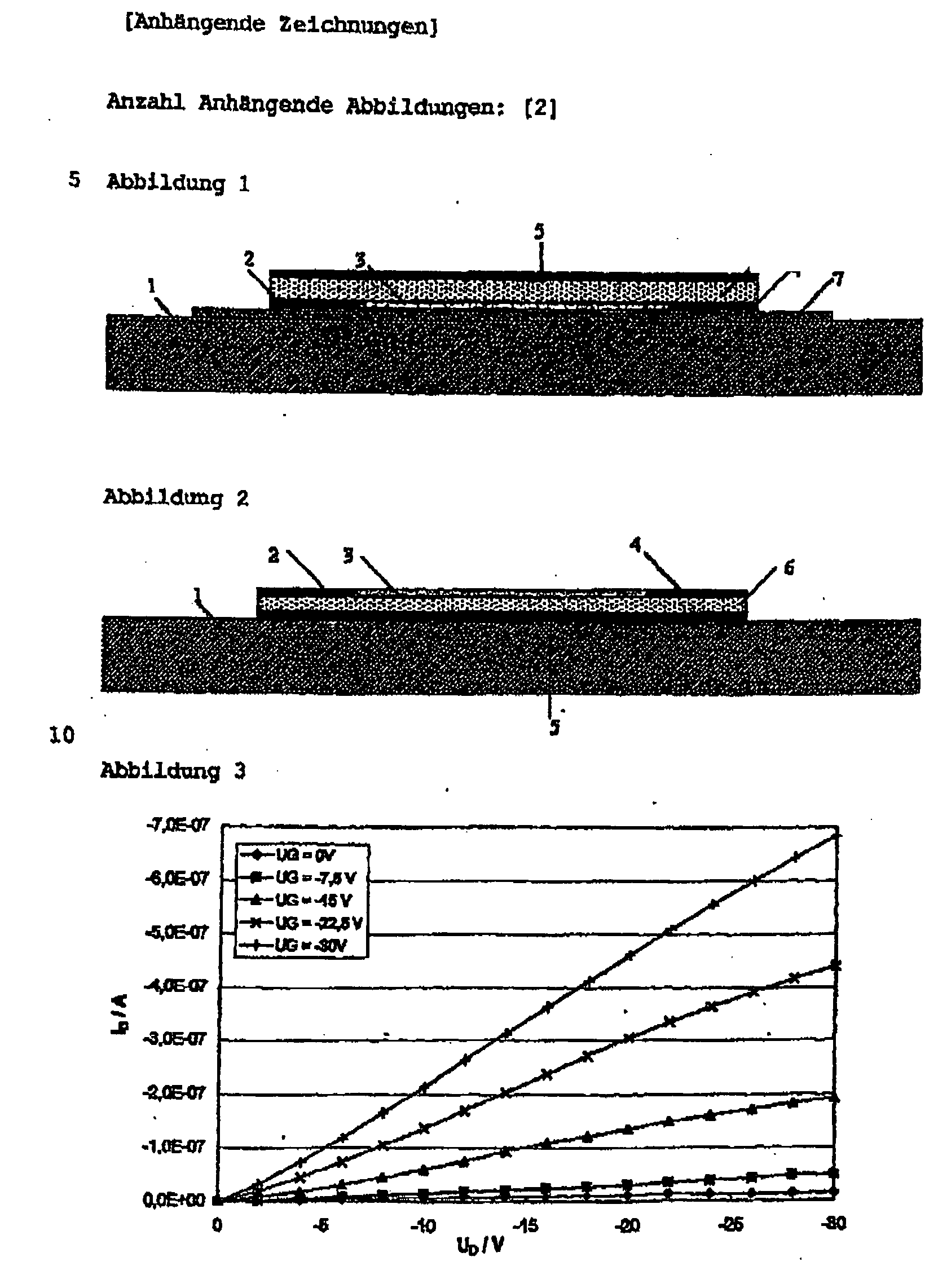
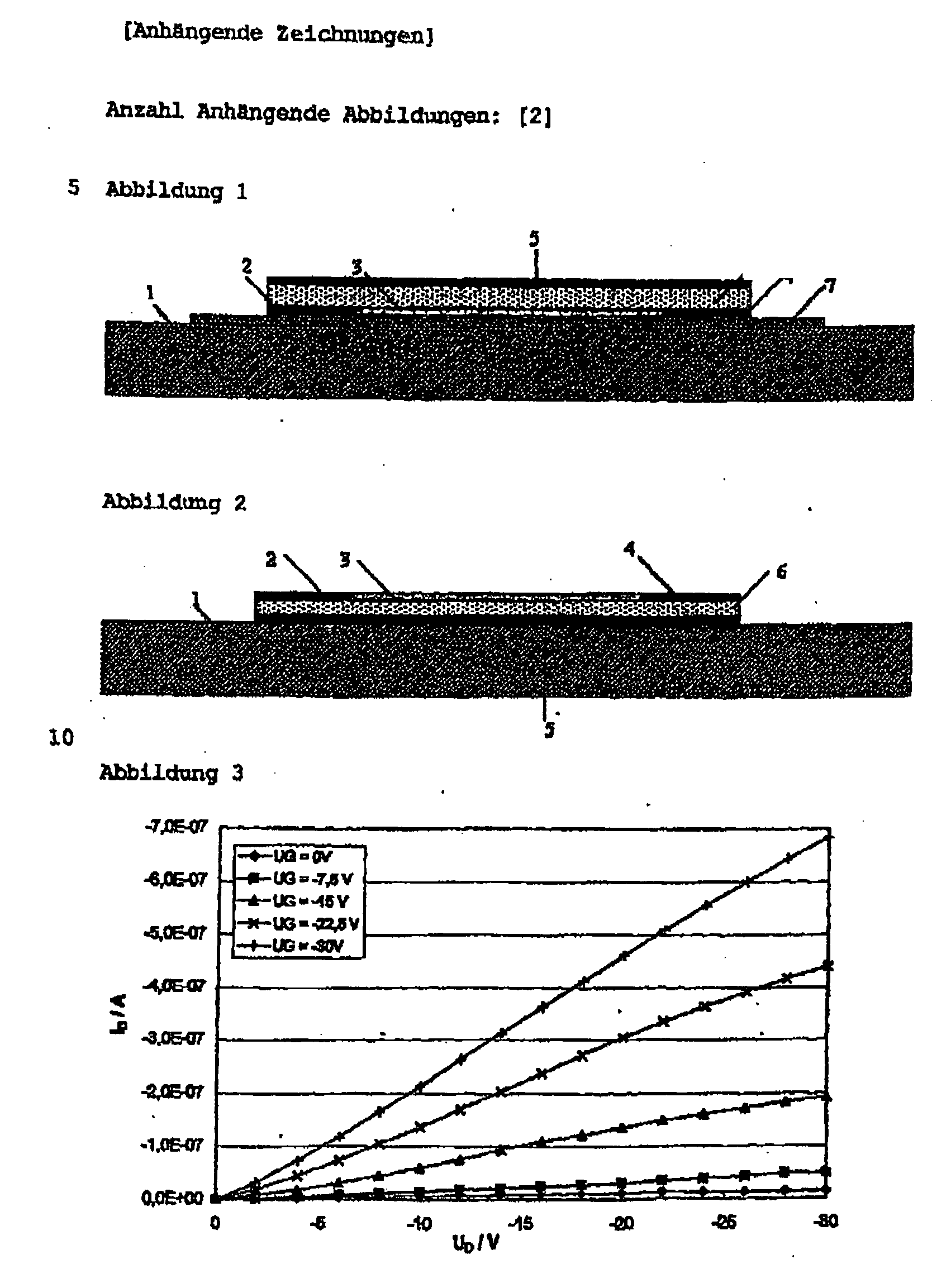
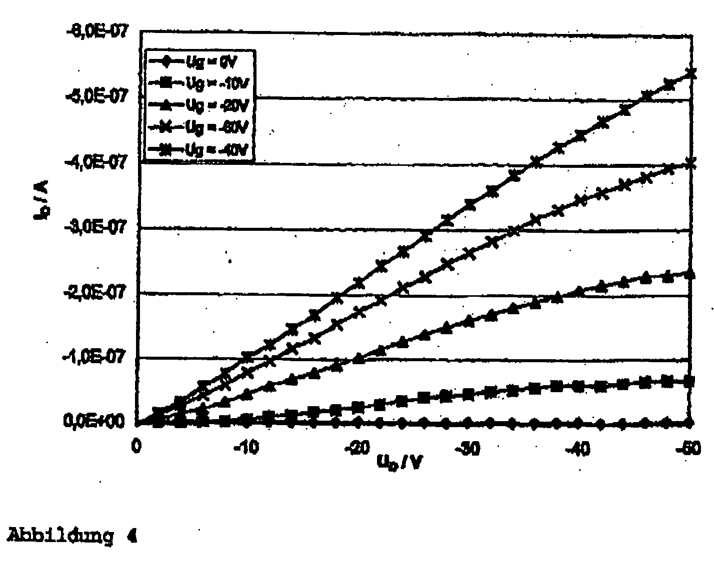
[0015]This example refers to the realization of the invention as shown in FIG. 2. A layer of the conductive polymer polyethylene dioxythiophen (Baytron) is applied by doctoring to an ABS-plate of 1 mm thickness as a plastic body 1. Said layer is structurized by selective laser abrasion with an excimer laser so that the gate electrodes 5 are obtained. Upon said layer and in order to generate the (insulation) protective layer 6, a layer of an alcoholic polyvinyl phenol solution containing a cross-linker is applied by spinning at 2000 r.p.m. Subsequently the polyvinyl phenol layer is tempered for 3 hours at 70° C. Over it, a thin gold layer (about 20 nm) is sputtered, out of which, in turn, the source-drain electrodes 2, 4 are generated by an excimer laser. Finally, the semiconductor layer 3 is applied by spinning up a 0.25% poly-3-hexylthiophen solution in toluol. The output characteristic of a field-effect transistor produced in such a way is shown in FIG. 4.


PUM

PropertyMeasurementUnit
temperaturesaaaaaaaaaa
temperatureaaaaaaaaaa

Abstract

The invention relates to the production of organic field-effect transistors (OFETs), solar cells or light-emitting diodes (OLEDs) and circuits based thereon on the surface of solvent- and/or temperature-sensitive plastics, e.g. thermoplastic injection-moulded bodies. A protective layer, which comprises a polymer compound, such as polyacrylate, polyphenol, melamine resin or polyester resin, which is applied from an aqueous-alcoholic solution or without solvent to the substrate surface or one of the function-determining layers of the electronic semiconductor component in a low-temperature process at temperatures of less than 100° C. and dried, protects the substrate against undesirable action of solvents and may simultaneously serve as a planarization layer and/or as as electrical insulation layer.

Description

[0001]The invention relates to the manufacture of organic field-effect transistors (OFETs), solar cells, or light emitting diodes (OLEDs) and circuits based thereon on the surface of solvent- and / or temperature-sensitive plastics, for example, thermo-plastic injection molded bodies. Furthermore, the invention relates to electronic components produced by said method.PRIOR ART[0002]In the last years organic semiconductor components have obtained an increasing importance also due to economical aspects. So it is possible to easily produce and, hence, by low costs, for example, organic field-effect transistors (OFETs) by simple methods on various substrates such as silicon, glass, polyester foils (PET, PEN), or polyimide foils (C. J. Drury, C. M. J. Mutsaers, C. M. Hart, M. Matters and D. M. de Leeuw: Appl. Phys. Lett. 73 (1998), 108; F. Eder, H. Klauk M. Halik, U. Zschieschang, G. Schmid and C. Dehm, Appl. Phys. Lett. 84 (2004), 2673; J. Ficker, A. Ullmann, W. Fix, H. Rost and W. Clemen...

Claims


Application Information

Patent Timeline
Patent Type & Authority Applications(United States)
IPC IPC(8): H01L51/00H01L31/18H01L21/02H01L31/00H01J1/62
CPCH01L51/004H01L51/0043H01L51/0097H01L51/0516Y02E10/549H01L51/0545H01L51/52H01L51/5237H01L51/0541Y02P70/50H10K85/141H10K85/151H10K77/111H10K10/468H10K10/466H10K10/464H10K50/80H10K50/844H01L2924/1307H10K50/84
Inventor SCHRODNER, MARIOSCHULTHEIS, KARINSCHACHE, HANNES
Owner THURINGISCHES INSTITUT FUR TEXTIL & KUNST FORSCHUNG
Why Eureka
Try Eureka