Group iii nitride semiconductor crystal substrate and semiconductor device

a semiconductor crystal substrate and nitride technology, applied in the direction of chemically reactive gases, polycrystalline material growth, crystal growth process, etc., can solve the problems of further noticeable problems, difficult to control the resistivity of the group, and difficult to control the concentration of silicon in the doping gas, so as to prevent the degradation of the resistivity in the plane. , the effect of resistivity reduction

Active Publication Date: 2009-05-21
SUMITOMO ELECTRIC IND LTD
View PDF30 Cites 17 Cited by
  • Summary
  • Abstract
  • Description
  • Claims
  • Application Information

AI Technical Summary

Benefits of technology

[0014]In view of the foregoing, an object of the present invention is to provide a group III nitride semiconductor crystal substrate, allowing the resistivity to be reduced and preventing degradation in the resistivity in-plane distribution.

Problems solved by technology

Moreover, the expectation of covering the two competing demands of high breakdown voltage and low loss, i.e. low ON-state resistance, that was difficult in conventional Si power devices, has attracted attention in the application to power devices.
It was difficult to control the concentration of silicon in the doping gas if the doping gas directed to supplying silicon was decomposed or caused reaction prior to arriving at the underlying substrate.
Therefore, it was difficult to control the resistivity of the group III nitride semiconductor crystal with silicon as a dopant.
Particularly, this problem was further noticeable when HVPE was employed since the decomposition of the doping gas and / or reaction with another gas was significant due to the entire heating of the reaction tube.
However, the concentration distribution of the doping gas supplied to the underlying substrate will be degraded if the doping gas is supplied at high rate, leading to significant degradation in the in-plane distribution of the resistivity in the group III nitride semiconductor crystal.
Thus, there was a problem that the property such as the ON-resistance is degraded in the case where the resistivity is not regulated and a semiconductor device is fabricated employing a group III nitride semiconductor crystal substrate of high resistivity.
Further, in the case where a semiconductor device is fabricated employing a group III nitride semiconductor crystal substrate having poor resistivity in-plane distribution, the yield was degraded since the property such as the ON-resistance of the semiconductor device will vary.

Method used


Image

  • Group iii nitride semiconductor crystal substrate and semiconductor device
  • Group iii nitride semiconductor crystal substrate and semiconductor device
  • Group iii nitride semiconductor crystal substrate and semiconductor device

Examples


first embodiment

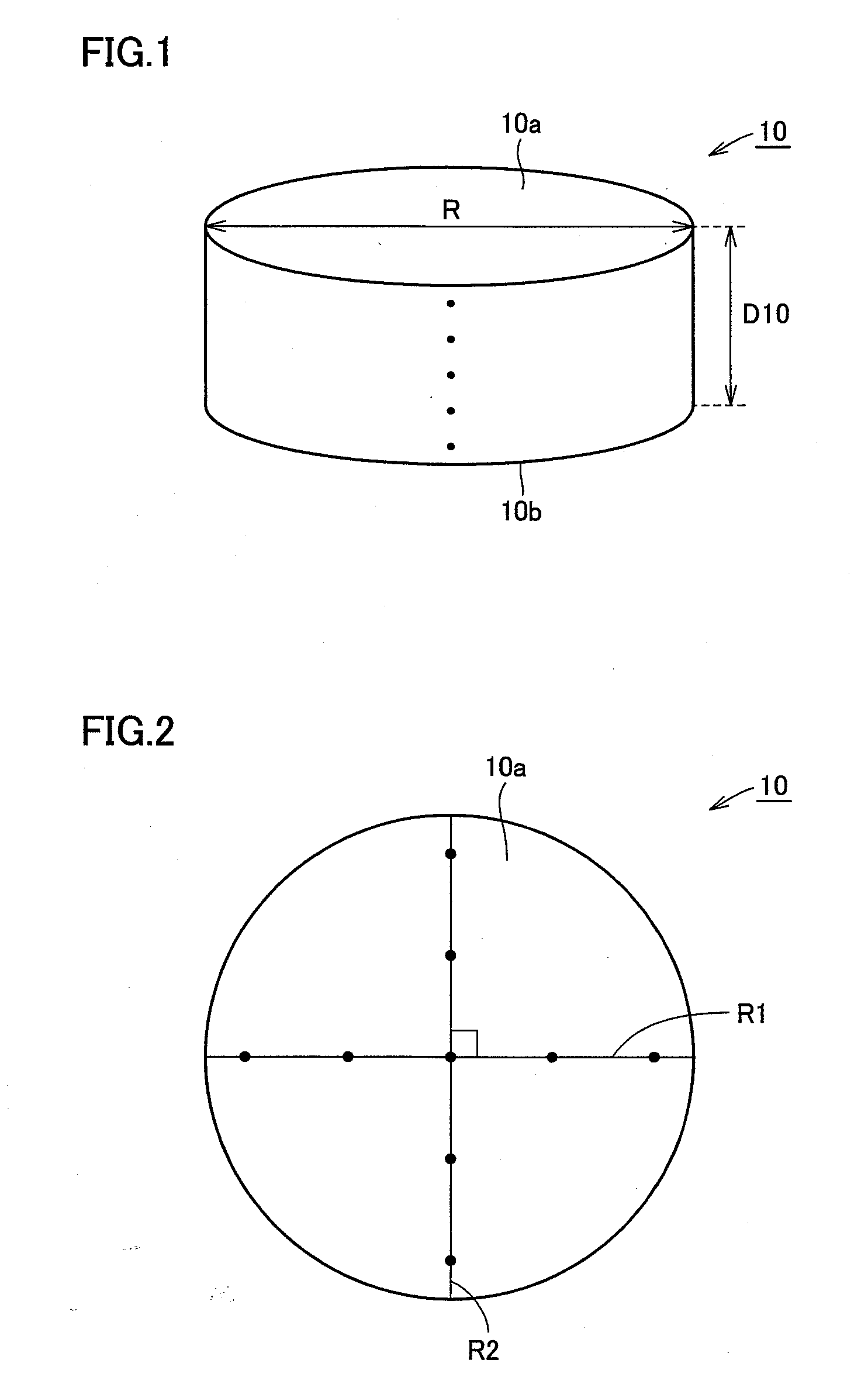
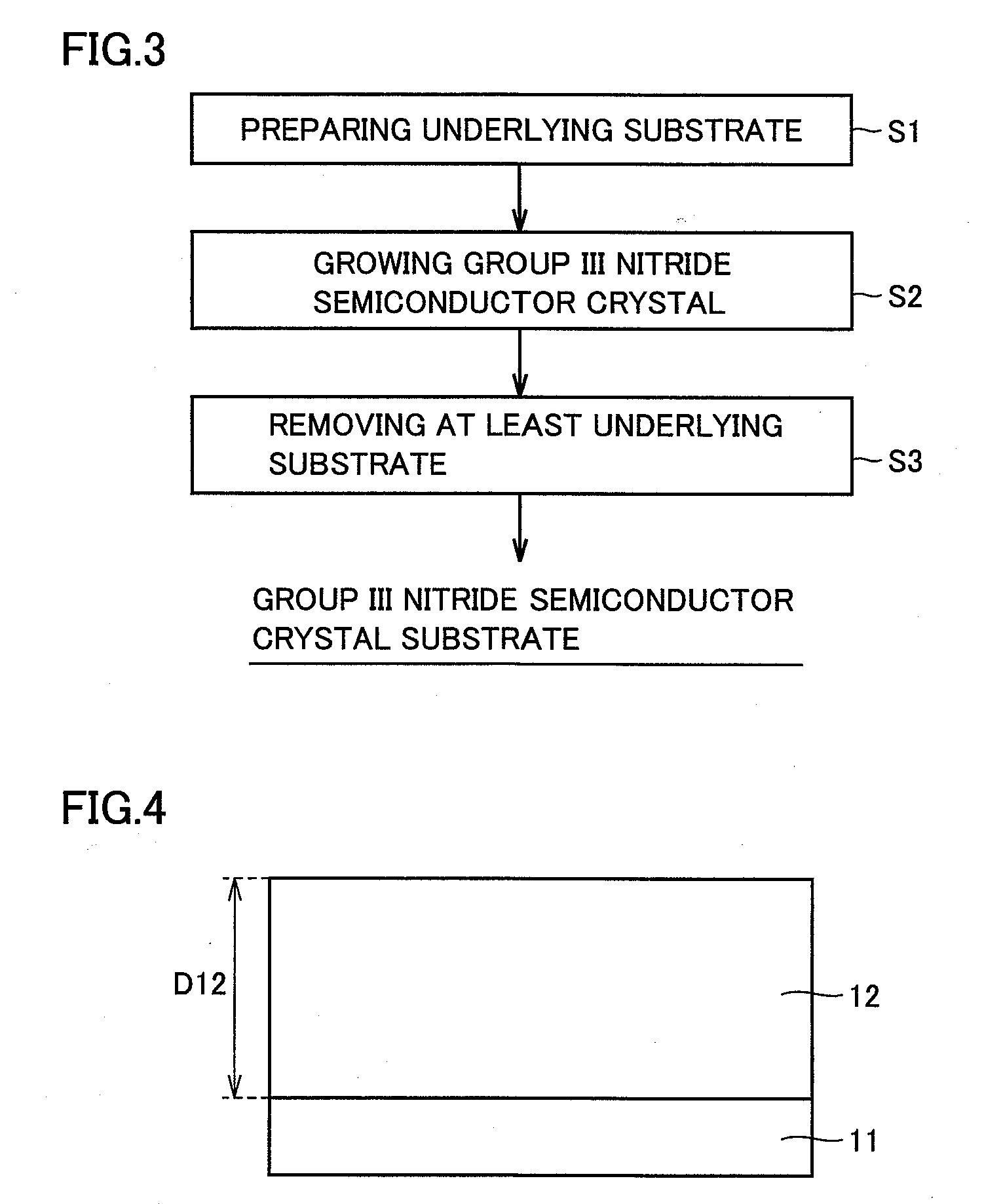
[0062]A group III nitride semiconductor crystal substrate according to an embodiment of the present invention will be described hereinafter with reference to FIGS. 1 and 2. As shown in FIGS. 1 and 2, a group III nitride semiconductor crystal substrate 10 is formed of a group III nitride semiconductor crystal 12 (refer to FIG. 4) having silicon doped as the impurity. Group III nitride semiconductor crystal substrate 10 includes a main face 10a.

[0063]As shown in FIGS. 1 and 2, a group III nitride semiconductor crystal substrate 10 of the present embodiment has a diameter R that is at least 25 mm and not more than 160 mm, preferably at least 45 mm and not more than 130 mm. A diameter R of at least 25 mm is advantageous in that the crystallinity of group III nitride semiconductor crystal substrate 10 is rendered favorable since the occurrence of a different plane orientation at main face 10a is prevented. In the case where diameter R is at least 45 mm, the crystallinity of group III ni...

second embodiment

[0127]A group III nitride semiconductor crystal substrate according to a second embodiment of the present invention is similar to group III nitride semiconductor crystal substrate 10 of the first embodiment shown in FIGS. 1 and 2. The fabrication method of a group III nitride semiconductor crystal substrate of the second embodiment differs from the fabrication method of a group III nitride semiconductor crystal of the first embodiment.

[0128]Specifically, the fabrication method of the present embodiment differs from the fabrication method of the first embodiment in that silicon tetrachloride gas is used as the doping gas to grow a group III nitride semiconductor crystal.

[0129]In detail, group III nitride semiconductor crystal 12 doped with silicon by using silicon tetrachloride gas as the doping gas is grown on underlying substrate 11 by vapor phase growth (step S2). In the present embodiment, silicon tetrachloride gas alone is employed for the doping gas. Elements differing from tho...

third embodiment

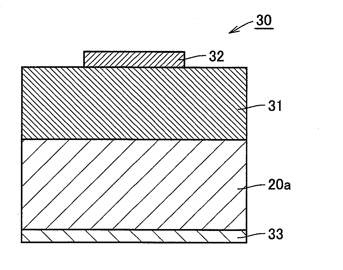
[0147]A group III nitride semiconductor crystal according to a third embodiment will be described with reference to FIG. 11.

[0148]As shown in FIG. 11, a group III nitride semiconductor crystal substrate 20a of the present embodiment is basically similar to group III nitride semiconductor crystal substrate 10 of the first embodiment shown in FIG. 1, provided that the thickness D20a is at least 100 μm and not more than 1000 μm.

[0149]Thickness D20a of group III nitride semiconductor crystal substrate 20a is at least 100 μm and not more than 1000 μm, preferably at least 60 μm and not more than 300 μm. In the case where thickness D20a is at least 100 μm, there can be obtained a group III nitride semiconductor crystal substrate 20a having generation of a crack during handling prevented. In the case where thickness D20a is at least 60 μm, a group III nitride semiconductor crystal substrate 20a having generation of a crack further prevented is obtained. In the case where thickness D20a is n...


PUM

PropertyMeasurementUnit
diameteraaaaaaaaaa
diameteraaaaaaaaaa
thicknessaaaaaaaaaa

Abstract

A group III nitride semiconductor crystal substrate has a diameter of at least 25 mm and not more than 160 mm. The resistivity of the group III nitride semiconductor crystal substrate is at least 1×10⁻⁴ Ω·m and not more than 0.1 Ω·cm. The resistivity distribution in the diameter direction of the group III nitride semiconductor crystal is at least −30% and not more than 30%. The resistivity distribution in the thickness direction of the group III nitride semiconductor crystal is at least −16% and not more than 16%.

Description

BACKGROUND OF THE INVENTION[0001]1. Field of the Invention[0002]The present invention relates to a group III nitride semiconductor crystal substrate and a semiconductor device.[0003]2. Description of the Background Art[0004]Gallium nitride (GaN) type semiconductor materials are known to have superior properties such as a large bandgap that is approximately 3 times that of silicon (Si), a high breakdown electric field that is approximately 10 times that of silicon, and also a high saturation electron velocity. Research and development of the gallium nitride type semiconductor material for use in devices of high frequency and high power output in the field of radio communication are actively in progress, and has already come to the stage of practical use in devices directed to base stations for cellular phones. Moreover, the expectation of covering the two competing demands of high breakdown voltage and low loss, i.e. low ON-state resistance, that was difficult in conventional Si powe...

Claims


Application Information

Patent Timeline
Patent Type & Authority Applications(United States)
IPC IPC(8): H01L29/20H01L33/32
CPCC30B25/02H01L29/2003C30B29/403
Inventor OKAHISA, TAKUJIKAWASE, TOMOHIROUEMURA, TOMOKINISHIOKA, MUNEYUKIARAKAWA, SATOSHI
Owner SUMITOMO ELECTRIC IND LTD
Why Eureka
Try Eureka