
Resist Underlayer Coating Forming Composition for Forming Photo-Crosslinking Cured Resist Underlayer Coating

a technology of resist and underlayer coating, applied in the direction of photosensitive materials, instruments, photomechanical equipment, etc., can solve the problems of difficult to apply organic materials for anti-reflective coating on a substrate having a high aspect ratio, etc., to achieve uniform film thickness, good photoresist pattern, and high dry etching rate

Active Publication Date: 2009-05-21
NISSAN CHEM IND LTD
View PDF20 Cites 19 Cited by
  • Summary
  • Abstract
  • Description
  • Claims
  • Application Information

AI Technical Summary

Benefits of technology

The present invention relates to a composition for forming an underlayer coating between a semiconductor substrate and a photoresist in a lithography process of the manufacture of semiconductor devices. The composition should be applied by light irradiation and should have properties such as filling properties, flattening properties, and anti-reflective properties. The invention also provides a method for forming the underlayer coating and a method for forming a photoresist pattern using the composition. The invention aims to solve problems related to interconnection delay and poisoning effect of photoresist layers in the manufacture of semiconductor devices.

Problems solved by technology

Along with this change, influences of random reflection and standing wave of actinic rays from a substrate have become serious problems.
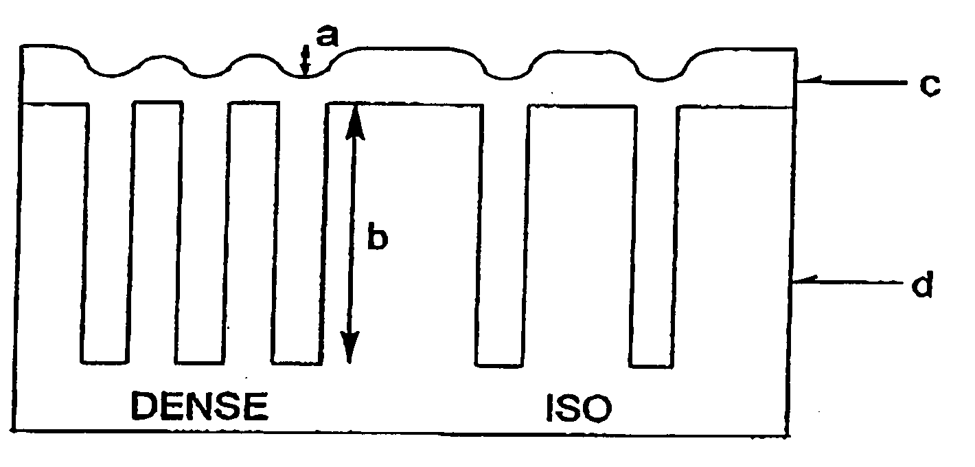
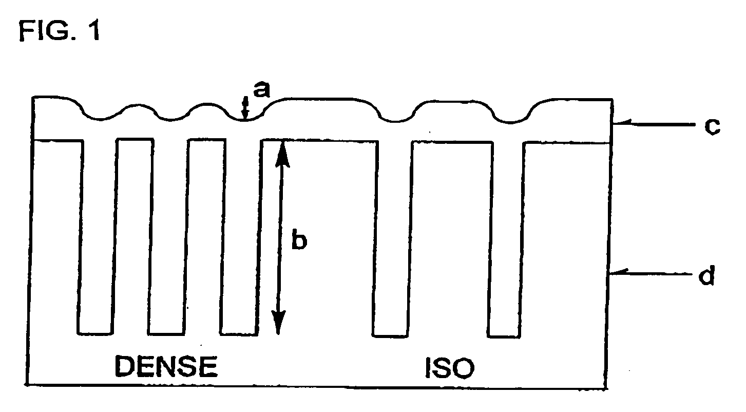
However, it is difficult to apply organic material for anti-reflective coating on a substrate having a high aspect ratio, and in recent years, material with particular emphasis on filling property or flattening property has been developed (see, for example Patent Documents 2, 3, 4 and 5).
On the other hand, the above-mentioned organic underlayer coating is formed by applying an underlayer coating forming composition on a semiconductor substrate, and then heating the semiconductor substrate at a high temperature of about 170° C. to 200° C. Therefore, components with a low molecular weight contained in the underlayer coating forming composition are volatilized or sublimated on heating at the high temperature, and this causes problems that the volatized or sublimated components adhere on peripheral apparatuses and thus the apparatuses are polluted.
Further, it becomes problems that the components adhered to the apparatuses fall on the semiconductor substrate and it exerts a harmful Influence on patter formation.

Method used


Image

  • Resist Underlayer Coating Forming Composition for Forming Photo-Crosslinking Cured Resist Underlayer Coating
  • Resist Underlayer Coating Forming Composition for Forming Photo-Crosslinking Cured Resist Underlayer Coating
  • Resist Underlayer Coating Forming Composition for Forming Photo-Crosslinking Cured Resist Underlayer Coating

Examples


example 1

[0100]In 25.87 g of propylene glycol monomethyl ether, 5 g of a photopolymerization compound: pentaerythritol tetramethacrylate (manufactured by Sigma-Aldrich Japan K.K., trade name: FW352), 0.25 g of a photopolymerization initiator triphenylsulfonium trifluoromethane sulfonate (manufactured by Midori Kagaku Co., Ltd., trade name: TPS105) and 0.05 g of a surfactant (manufactured by Dainippon Ink and Chemicals Incorporated, trade name; Megafac R-30) were added to prepare a solution of 17 mass % (solid content concentration). Then, the solution was filtered through a micro filter made of polyethylene having a pore size of 0.2 μm to prepare a solution of an underlayer coating forming composition.

example 2

[0101]In 25.87 g of propylene glycol monomethyl ether, 5 g of a photopolymerization compound: bis(4-glycidyloxyphenyl)methane (manufactured by Sigma-Aldrich Japan K.K., trade name: FW312), 0.25 g of a photopolymerization initiator: triphenylsulfonium trifluoromethane sulfonate (manufactured by Midori Kagaku Co., Ltd., trade name: TPS105) and 0.05 g of a surfactant (manufactured by Dainippon Ink and Chemicals Incorporated, trade name: Megafac R-30) were added to prepare a solution of 17 mass % (solid content concentration). Then, the solution was filtered through a micro filter made of polyethylene having a pore size of 0.2 μm to prepare a solution of an underlayer coating forming composition.

example 3

[0102]In 27.10 g of propylene glycol monomethyl ether, 5 g of a photopolymerization compound: bisphenol-A-propoxylate diglycidyl ester (manufactured by Sigma-Aldrich Japan K.K., trade name: FW457), 0.50 g of a photopolymerization initiator: triphenylsulfonium trifluoromethane sulfonate (manufactured by Midori Kagaku Co., Ltd., trade name: TPS105) and 0.05 g of a surfactant (manufactured by Dainippon Ink and Chemicals Incorporated, trade name: Megafac R-30) were added to prepare a solution of 17 mass % (solid content concentration). Then, the solution was filtered through a micro filter made of polyethylene having a pore size of 0.2 μm to prepare a solution of an underlayer coating forming composition.


PUM

PropertyMeasurementUnit
aspect ratioaaaaaaaaaa
wavelengthaaaaaaaaaa
temperatureaaaaaaaaaa

Abstract

There is provided an underlayer coating that is used as an underlayer of photoresists in lithography process of the manufacture of semiconductor devices and that has a high dry etching rate in comparison to the photoresists, does not intermix with the photoresists, and is capable of flattening the surface of a semiconductor substrate having holes of a high aspect ratio; and an underlayer coating forming composition for forming the underlayer coating.The underlayer coating forming composition for forming by light irradiation an underlayer coating used as an underlayer of a photoresist in a lithography process of the manufacture of semiconductor devices, comprises a polymerizable substance and a photopolymerization initiator.

Description

TECHNICAL FIELD[0001]The present invention relates to a composition for forming an underlayer coating between a semiconductor substrate and a photoresist. Specifically, the present invention relates to an underlayer coating forming composition for forming by light irradiation an underlayer coating used as an underlayer of a photoresist in a lithography process of the manufacture of semiconductor devices. The present invention also relates to a method for forming an underlayer coating by use of the underlayer coating forming composition, and a method for forming a photoresist pattern.BACKGROUND ART[0002]Conventionally, In the manufacture of semiconductor devices, micro-processing by lithography using a photoresist has been carried out. The micro-processing is a processing method comprising forming a thin coating of a photoresist on a semiconductor substrate such as a silicon wafer or the like, irradiating actinic rays such as ultraviolet rays through a mask pattern on which a pattern...

Claims


Application Information

Patent Timeline
Patent Type & Authority Applications(United States)
IPC IPC(8): G03F7/20G03F7/004B05D3/06B32B37/02
CPCG03F7/091H01L21/0271G03F7/11G03F7/161
Inventor TAKEI, SATOSHISHINJO, TETSUYAHIDAKA, MOTOHIKO
Owner NISSAN CHEM IND LTD
Learn More