Thin film field effect transistor and electroluminescence display using the same

a field effect transistor and thin film technology, applied in the direction of basic electric elements, electrical equipment, semiconductor devices, etc., can solve the problems of insufficient performance, low heat resistance, and difficulty in forming transistors directly on resin substrates

Inactive Publication Date: 2009-05-28
UDC IRELAND
View PDF2 Cites 59 Cited by
  • Summary
  • Abstract
  • Description
  • Claims
  • Application Information

AI Technical Summary

Benefits of technology

[0036]The active layer in the present invention preferably further contains a second amorphous oxide, wherein an electron carrier concentration of the second amorphous oxide tends to decrease together with lowering of a temperature thereof from room temperature, and the second amorphous oxide has an activation energy of less than 0.04 eV. When the activation energy in the second amorphous oxide according to the invention exceeds 0.04 eV, it exhibits properties that are not different from those of the first amorphous oxide, whereby the effects of the second amorphous oxide are not sufficiently exerted.
[0037]The first amorphous oxide and the second amorphous oxide in the present invention can be used in a two-layer structure. In this case, preferably, the active layer has at least a first layer composed of an amorphous oxide having an activation energy of from 0.04 eV to 0.10 eV and a second layer composed of an amorphous oxide having an activation energy of less than 0.04 eV, wherein the second layer is in contact with the gate insulating layer, and the first layer is disposed so as to be electrically connected between the second layer and at least one of the source electro

Problems solved by technology

However, fabrication of the transistors using the silicon thin films described above requires a thermal treatment process at a relatively high temperature, and it is difficult to form the transistors directly on a resin substrate which is generally low in heat resistance.
However, in the case of using a TFT formed using a-IGZO, as, for example, a drive circuit of a display, there are the problems in that

Method used


Image

  • Thin film field effect transistor and electroluminescence display using the same
  • Thin film field effect transistor and electroluminescence display using the same
  • Thin film field effect transistor and electroluminescence display using the same

Examples


example 1

1. Preparation of Active Layer

[0092](Preparation of Amorphous Oxide)

[0093]

[0094]Using a polycrystalline sintered body having a composition of InGaZnO4 as a target, RF magnetron sputtering vacuum deposition was performed in the presence of argon gas (Ar), while maintaining the total pressure of gas of 0.37 Pa and component pressure of oxygen (O2) of 0.0005 Pa, under a condition of RF power of 200 W. During the process, the moisture partial pressure was 1.0×10⁻⁴ Pa. As a substrate, a non-alkali glass substrate ((#1737, manufactured by Corning) was used. The center of gravity of the substrate was located at 90 nm just above the center of gravity of the target. The line connecting the center of gravity of the substrate plane and the center of gravity of the target plane had an angle of 90° against the target plane.

[0095]

[0096]Deposition was performed under similar conditions to those in the Condition 1 except that the partial pressure of O2 was changed to 0.001 Pa.

[0097]

[0098]Deposition...

example 2

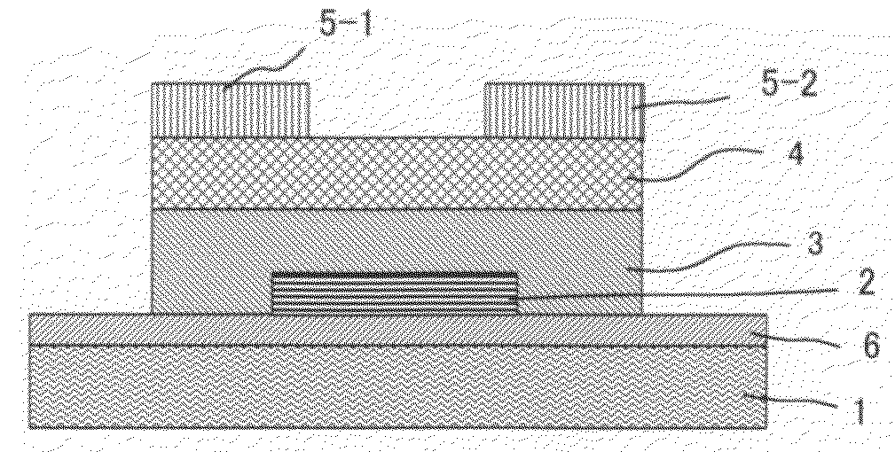
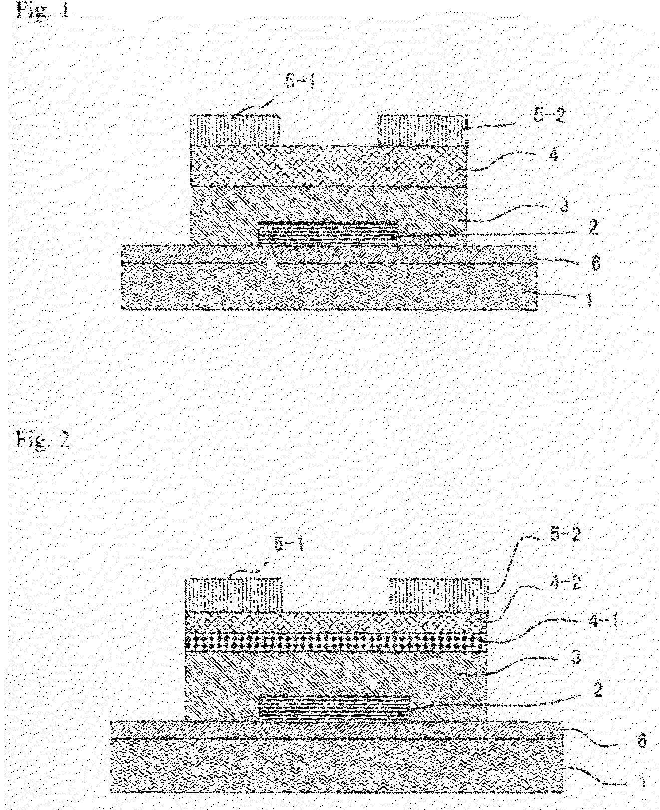
[0152]In the configuration of TFT in Example 1, the configuration was changed to that shown in FIG. 2, in which two active layers different in carrier concentration are laminated.

[0153]First region of active layer: a layer of the amorphous oxide prepared according to the Condition 3 was provided at a thickness of 40 nm.

[0154]Second region of active layer: a layer of the amorphous oxide prepared according to the Condition 1 was provided at a thickness of 10 nm.

[0155]The obtained TFT exhibited further excellent performance with Ids of 5×10⁻¹¹ A and electron mobility of 13.8 cm2 / Vs.

example 3

[0156]In the configuration of TFT in Example 1, a co-deposition layer of the following amorphous oxides was used as the active layer.

[0157]The amorphous oxide prepared according to the Condition 3 and the amorphous oxide prepared according to the Condition 1 were co-deposited in a ratio of 4:1 (by weight ratio). The deposition thickness was 50 nm.

[0158]The obtained TFT exhibited further excellent performance with Ids of 7×10⁻¹¹ A and electron mobility of 12.5 cm2 / Vs.


PUM


Abstract

A thin film field effect transistor that has on a substrate, at least a gate electrode, a gate insulating layer, an active layer, a source electrode and a drain electrode, wherein the active layer includes an amorphous oxide, a carrier concentration of the amorphous oxide decreases together with lowering of a temperature thereof from room temperature, and the amorphous oxide has an activation energy of from 0.04 eV to 0.10 eV is provided. A thin film field effect transistor having high mobility and a high ON-OFF ratio, and a high-gradation electroluminescence display using the same are provided.

Description

CROSS-REFERENCE TO RELATED APPLICATION[0001]This application claims priority under 35 USC 119 from Japanese Patent Application Nos. 2007-304879 and 2008-247625, the disclosures of which are incorporated by reference herein.BACKGROUND OF THE INVENTION[0002]1. Field of the Invention[0003]The present invention relates to a thin film field effect transistor and an electroluminescence display using the same. Particularly, it relates to a thin film field effect transistor in which an amorphous oxide semiconductor is used for an active layer, and an electroluminescence display using the same.[0004]2. Description of the Related Art[0005]In recent years, flat panel displays (FPDs) have been put to practical use, due to the progress made in liquid crystal and electroluminescence (EL) technologies, etc. Especially, an organic electroluminescence element (hereinafter sometimes referred to as an “organic EL element”) formed using a thin film material which emits light by excitation due to applic...

Claims


Application Information

Patent Timeline
IPC IPC(8): H01L29/22
CPCH01L29/7869
Inventor MATSUNAGA, ATSUSHI
Owner UDC IRELAND
Why Eureka
Try Eureka