Silicon carbide mos field-effect transistor and process for producing the same

a field-effect transistor and silicon carbide technology, applied in the direction of basic electric elements, electrical apparatus, semiconductor devices, etc., can solve the problems of reducing the efficiency of the field-effect transistor, so as to achieve low on-resistance, high blocking voltage, and high accuracy

Inactive Publication Date: 2009-05-28
NAT INST OF ADVANCED IND SCI & TECH
View PDF4 Cites 28 Cited by
  • Summary
  • Abstract
  • Description
  • Claims
  • Application Information

AI Technical Summary

Benefits of technology

[0016]As described above, this invention manifests the following effect.
[0017]The inventions set forth in claim 1 and claim 2 enable realizing an SiC vertical MOSFET exhibiting low On-resistance and high blocking voltage by providing the low-concentration p-type deposition layer therein with a low-concentration channel region and interposing a comparatively thick deposition film between the gate oxide film and the high-concentration gate layer. The vertical MOSFET having a high blocking voltage of not less than 1500 V can be realized by properly selecting the impurity concentration and the thickness of an interposed n-type deposition layer (33).
[0018]The inventions set forth in claim 3 and claim 6 allow forming a second conduction type high-concentration gate layer with high accuracy and therefore facilitating refinement of cells and, consequently, enable increasing blocking voltage and decreasing loss of the SiC vertical MOSFET.
[0019]The inventions set forth in claim 4 and claim 6 relate to a configuration that invariably has a deposition film stacked on a deposition film and a method for the fabrication thereof and consequently allow enhancing the crystal quality of the channel region and decreasing the On-resistance of the SiC vertical MOSFET.
[0020]The invention set forth in claim 5 enables easy fabrication of the vertical MOSFET that exhibits high blocking voltage and low On-resistance.
[0021]The invention set forth in claim 8 allows improving the uniformity of an electric current in motion in the ON state and as well refining the cell to a size of about 15 μm owing to the effect of one kind of self-alignment action and therefore enables substantially decreasing the On-resistance of the vertical MOSFET.

Problems solved by technology

When SiC is used as a raw material the vertical MOSFET cannot be fabricated by the double diffusion method that is generally applied to Si.
This method, however, degrades electron mobility because numerous crystal defects induced by ion implantation remain, in the channel region and scatter the conduction electrons induced in the channel.
As a result, the product entails the problem that the On-resistance is far higher than the theoretical value thereof.
Even this configuration, however, entails problems that inhibit efforts directed toward further adding to blocking voltage and lowering On-resistance as described below.
The problem that this electric field gams in intensity in consequence of the increase of voltage even after the vertical channel part is pinched off and the dielectric breakdown of the gate oxide film in this part restrains the blocking voltage between the source and the dram to a low level also persists.
The deposition film on the layer exposed to implantation effected in such a high concentration as this is liable to have the solid-state properties thereof as a single crystal film conspicuously impaired.
The vertical MOSFET configuration proposed heretofore, however, is incapable of forming the low-concentration p-type deposition film in an increased thickness owing to the restriction imposed on the process followed in the fabrication thereof.
Any further addition to this thickness is difficult to obtain.

Method used


Image

  • Silicon carbide mos field-effect transistor and process for producing the same
  • Silicon carbide mos field-effect transistor and process for producing the same
  • Silicon carbide mos field-effect transistor and process for producing the same

Examples


embodiment 1

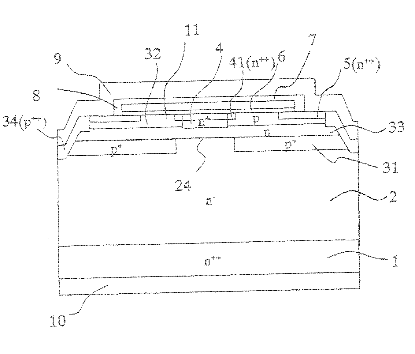
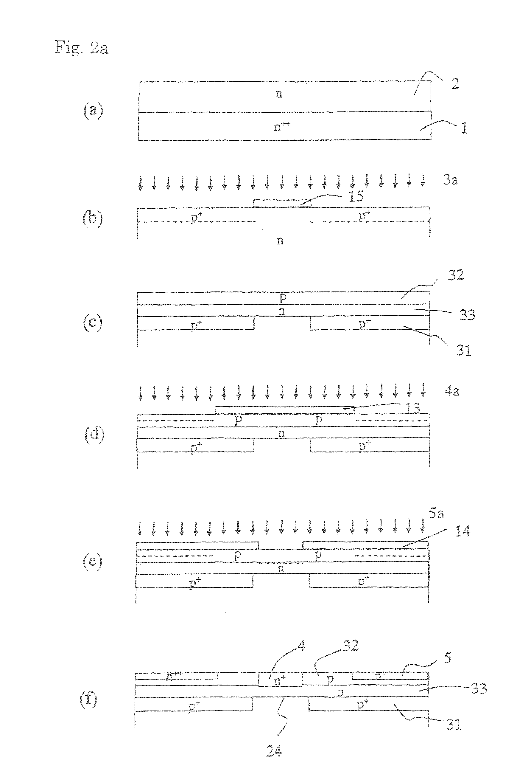
[0060]FIG. 1 is a cross section of the unit cell of a SiC vertical MOSFET in Embodiment 1 of this invention. In this configuration, an n-type drift layer 2 doped with nitrogen in a concentration of 5×1015 cm−3 is deposited in a thickness of 15 μm on an n-type SiC substrate 1 doped with nitrogen in a concentration of 5×1018 cm−3 and having a thickness of about 300 μm. A p-type layer 31 doped with aluminum in a concentration of 2×1018 cm−3 is formed across a depth of 0.5 μm from the surface thereof and the p-type layer 31 is provided with a partial depletion part 24 having a width of about 2.0 μm. An n-type layer 33 doped with nitrogen in a concentration of 1×1016 cm−3 is deposited in a thickness of 1.0 μm on the surface of the p-type layer 31 and the surface of the n-type drift layer 2 of the partial depletion part 24 and a p-type layer 32 doped with aluminum in a concentration of 5×1015 cm−3 is deposited in a thickness of 0.5 μm on the surface of the n-type layer 33. On the surface ...

embodiment 2

[0064]FIG. 3 is a cross section of the unit cell of an SiC vertical MOSFET in Embodiment 2 of this invention. In this configuration, the n-type drift layer 2 doped with nitrogen in a concentration of 5×1015 cm−3 was deposited in a thickness of 15 μm on the substrate 1 doped with nitrogen in a concentration of 5×1018 cm−3 and having a thickness of about 300 μm. The p-type layer 31 doped with aluminum in a concentration of 2×1018 cm−3 was deposited in a thickness of 0.5 μm on the resultant surface, and the p-type layer 31 was provided with a partial depletion part 24 having a width of about 2.0 μm. On the surface of the p-type layer 31 and the surface of the n-type drift layer 2 of the partial depletion part 24, the n-type layer 33 doped with nitrogen in a concentration of 1×1016 cm−3 was deposited in a thickness of 1.0 μm. Further, on the surface of the n-type layer 33, the p-type layer 32 doped with aluminum in a concentration of 5×1015 cm−3 was deposited in a thickness of 0.5 μm. O...

embodiment 3

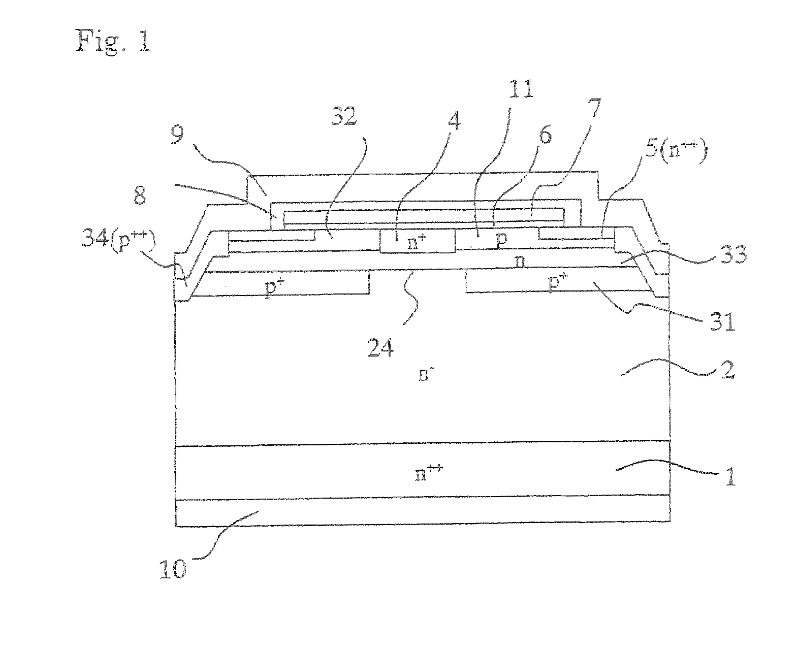
[0066]FIG. 4 is a cross section of the SiC vertical MOSFET in Embodiment 3 of this invention. In the drawing, the sites bearing the same reference numerals as in FIG. 1 designate the same parts and the basic configuration is identical with that of Embodiment 1 of FIG. 1 except that a high-concentration n-type layer 41 is disposed as parted on the opposite sides of the n-type base region 4. The high-concentration n-type layer 41 was simultaneously formed with the n-type source layer 5 and was equaled therewith in impurity concentration and depth from the surface and was given a length substantially equal to the partial depletion part 24. The provision of this layer was effective in preventing refinement of cells and concentration of an electric current because it enabled equalizing the two channel regions 11 contained in the unit cell in terms of length and imparting a prescribed relation to their relative positions. This operational effect may be well comprehended from the method of...


PUM


Abstract

In the SiC vertical MOSFET having a low-concentration p-type deposition film provided therein with a channel region and a base region resulting from reverse-implantation to n-type through ion implantation, dielectric breakdown of gate oxide film used to occur at the time of off, thereby preventing a further blocking voltage enhancement. This problem has been resolved by interposing of a low-concentration n-type deposition film between a low-concentration p-type deposition film and a high-concentration gate layer and selectively forming of a base region resulting from reverse-implantation to n-type through ion implantation in the low-concentration p-type deposition film so that the thickness of deposition film between the high-concentration gate layer and each of channel region and gate oxide layer is increased.

Description

TECHNICAL FIELD[0001]This invention relates to the configuration of a vertical MOSFET having a low On-resistance and a high voltage and using silicon carbide as raw material and a method for producing the same.BACKGROUND ART[0002]The single crystal of silicon carbide (SiC) possesses excellent solid state properties, such as a wide band gap, high dielectric breakdown strength and a large saturation drift velocity of electrons as compared with the single crystal of silicon (Si). By using SiC as a starting material, therefore, it is rendered possible to fabricate a semiconductor device for use with an electrical power of high blocking voltage and low resistance exceeding the limits on Si. SiC is further characterized by being capable of forming an insulating layer by thermal oxidation similarly to Si. These facts lead to a supposition that the fabrication of a vertical MOSFET having a high blocking voltage and a low On-resistance and using the single crystal of SiC as a raw material is...

Claims


Application Information

Patent Timeline
Patent Type & Authority Applications(United States)
IPC IPC(8): H01L29/78H01L21/3205H01L21/02
CPCH01L21/0465H01L29/0623H01L29/0653H01L29/0878H01L29/7828H01L29/1608H01L29/41766H01L29/66068H01L29/7802H01L29/1095
Inventor YATSUO, TSUTOMUHARADA, SHINSUKEOKAMOTO, MITSUOFUKUDA, KENJI
Owner NAT INST OF ADVANCED IND SCI & TECH
Why Eureka
Try Eureka