Photodiode, method for manufacturing such photodiode, optical communication device and optical interconnection module

a photodiode and photodiode technology, applied in semiconductor/solid-state device manufacturing, semiconductor devices, electrical apparatus, etc., can solve the problems of reducing the utilization efficiency of signal light, reducing the voltage of a reproduced signal that is detected, and difficult to achieve high sensitivity of this structure, etc., to achieve high yield, high efficiency, and efficient conversion of energy into photocarriers

Inactive Publication Date: 2009-05-28
NEC CORP
View PDF7 Cites 75 Cited by
  • Summary
  • Abstract
  • Description
  • Claims
  • Application Information

AI Technical Summary

Benefits of technology

[0029]The present invention realizes a high-speed and highly efficient photodetector that is capable of concentrating optical energy within a region having a wavelength size or a region smaller than the wavelength and that is capable of efficiently converting the energy to photocarriers to obtain an electric signal. Furthermore, the present invention realizes a manufacturing process for a photodiode with a high yield and at low cost even in the case of high degree integration.

Problems solved by technology

However, it is difficult for this structure to achieve high sensitivity because of the poor optical absorption efficiency on the surface layer of semiconductor, although it provides an enhanced response.
On the other hand, reducing the value of load resistance to shorten the time constant of the circuit causes a decrease in the voltage of a reproduced signal that is detected.
However, reducing the junction area is problematic because it causes a reduction in utilization efficiency of signal light, which results in degradation of the SN ratio of the reproduced signal.
The MSM-type optical detector is disadvantageous in that increasing the thickness of a semiconductor for the purpose of increasing quantum efficiency causes an increase in the propagation distance of photocarriers and resultantly causes a slow response.
However, these light receiving elements are problematic because reducing the radiation area of incident light in order to reduce the electric capacitance of the depletion layer leads to a reduction in the intensity of the detected signal and deterioration of the SN ratio.
However, this technique does not describe reducing the thickness and the area of a depletion layer in order to enhance response of photoelectric conversion.
Therefore, a high SN ratio can not be obtained even if propagating light from this optical transmission apparatus is radiated onto a light receiving element.
However, this structure does not realize a reduction in the junction area of the MSM junction and a resultant reduction in the element capacitance.
However, the optical detector using Si or SiGe generally shows a slow response due to a long carrier life time (˜1 to 10 μs) and a low optical absorption rate (˜10 to 100 / cm).
Furthermore, in the case of a compound semiconductor, a Schottky barrier type photodiode provides a high-speed response, but is problematic because the metal electrodes reduce the effective light receiving area and reduce sensitivity.
This structure can reduce the distance between the electrodes to achieve a high-speed response, but is problematic because it is difficult to achieve high sensitivity.
However, this process disadvantageously tends to cause a yield reduction in the device manufacturing process, as well as electrical short circuits between electrodes generated by lift-off residues.

Method used


Image

  • Photodiode, method for manufacturing such photodiode, optical communication device and optical interconnection module
  • Photodiode, method for manufacturing such photodiode, optical communication device and optical interconnection module
  • Photodiode, method for manufacturing such photodiode, optical communication device and optical interconnection module

Examples


example 1

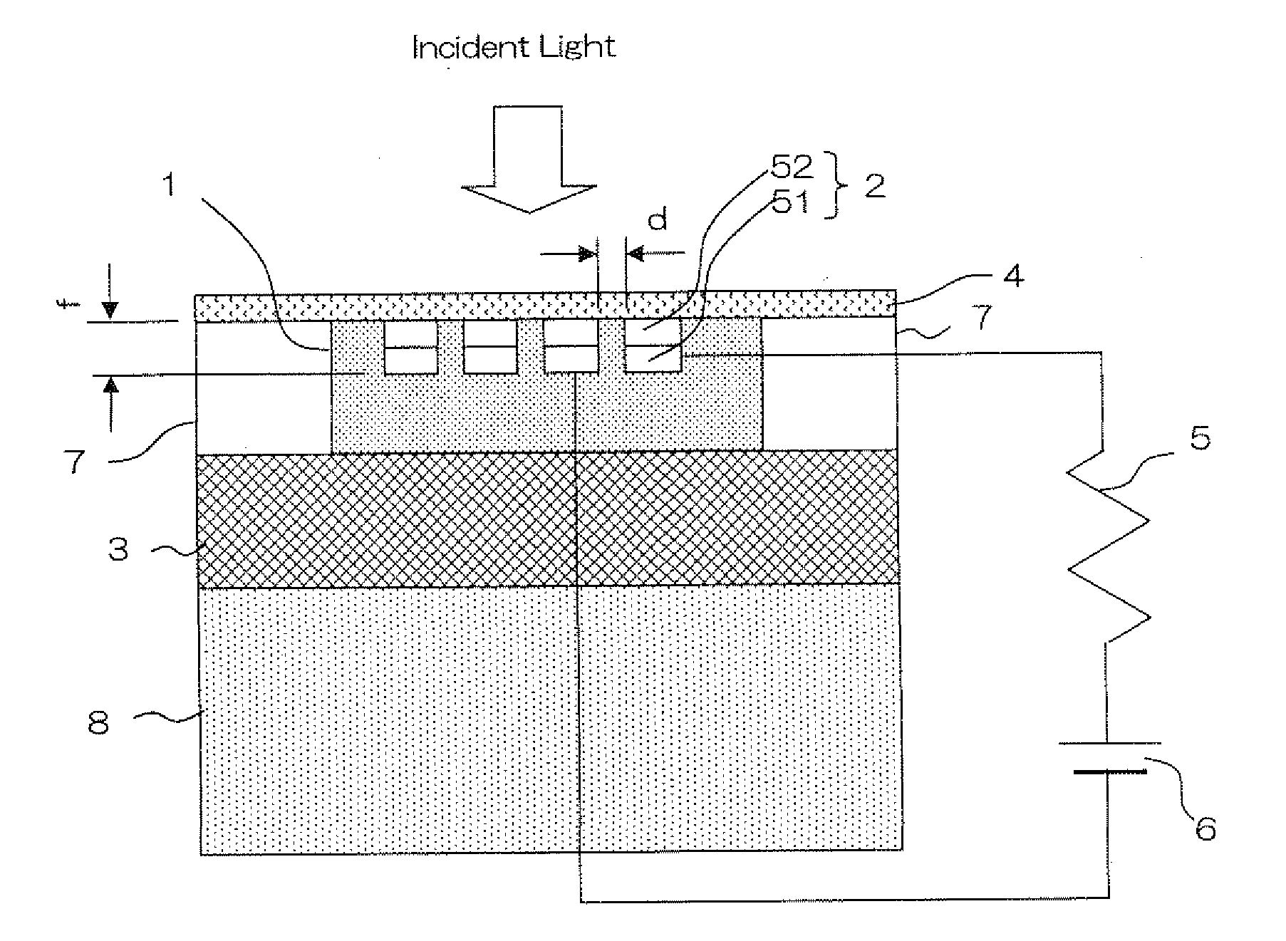
[0082]FIGS. 7 and 8 are a cross-sectional view and a plan view of an MSM photodiode according to a first example of the present invention, respectively. The MSM type photodiode forms metal-semiconductor-metal (MSM) junctions that are formed on part of semiconductor layer 1 having an insulated surface, such as an SOI (Silicon-on-Insulator). Interval d between metal electrodes 2 is less than wavelength λ of incident light and larger than 1 / 100 λ. Assuming n is the refractive index of semiconductor layer 1, metal electrodes 2 are embedded into semiconductor layer 1 at distance f that is less than λ / 2n measured from the surface of semiconductor layer 1. In order to induce surface plasmon, aluminum, silver, gold or copper or an alloy made up of two or more of the elements aluminum, silver, gold and copper is preferably used for metal electrode 2 (or at least second metal film 52). A seed film made of Cr, Ta, Ni etc. may also be used in order to form a Schottky junction. Furthermore, a se...

example 2

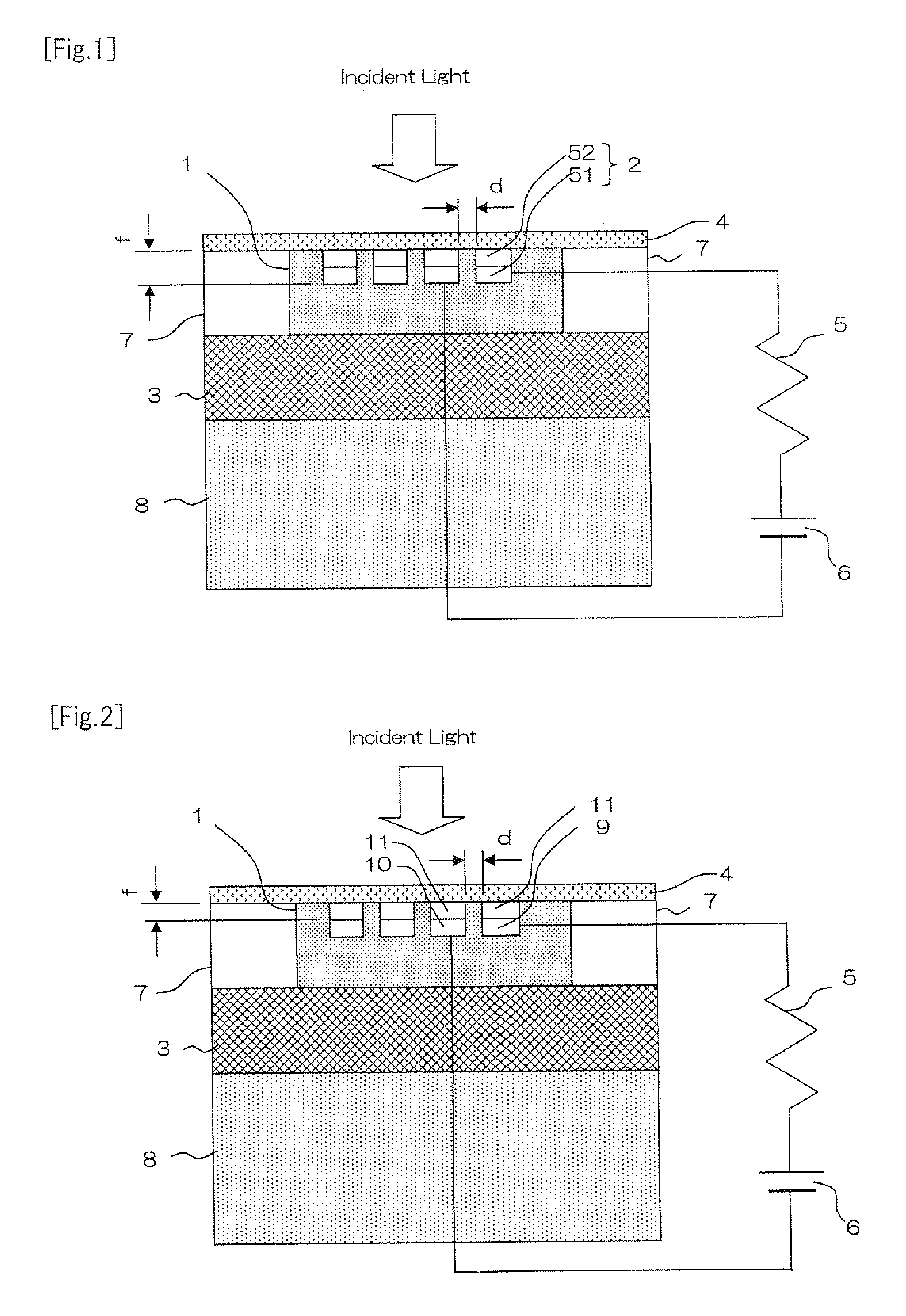
[0084]FIG. 10 is a cross-sectional view of a photodiode according to a second example of the present invention. Schottky electrodes 22 forming a Schottky junction are arranged at interval d on the surface of semiconductor layer 1. Schottky electrodes 22 are made of a conductive material that is capable of inducing surface plasmon. Opposite electrode layer 23 is formed on the side of base substrate 8 via a depletion layer (semiconductor layer 1) which serves as a light absorbing layer. Interval d of Schottky electrodes 22 is less than light wavelength 1. Assuming that n is the refractive index of semiconductor layer 11 Schottky electrodes 22 are embedded into semiconductor layer 1 at distance f that is less than λ / 2n.

[0085]An n+-Si layer that includes a dopant, such as P, with a dopant concentration of 1×1020 cm−3 or more may be used as opposite electrode layer 23 and an n-Si layer which serves as a light absorbing layer may be used as semiconductor layer 1. Semiconductor layer 1 req...

example 3

[0087]FIG. 11 is a cross-sectional view of a photodiode according to a third example of the present invention. A stack in which metal film 11 is deposited on p electrode 9 or n electrode 10 is disposed on the surface of semiconductor layer 1, forming at least one p-i-n junction. Interval d of metal films 11 deposited on p electrode 9 or n electrode 10 is designed to be less than wavelength λ of incident light and to be greater than 1 / 100 λ. Metal film 11 is made of a conductive material that is capable of inducing surface plasmon and metal film 11 is embedded into semiconductor layer 1 at distance f that is less than λ / 2n measured from the surface of semiconductor layer 1, where n is the refractive index of semiconductor layer 1. Metal film 11 is preferably made up of aluminum, silver, gold or copper or an alloy made up of two or more of the elements aluminum, silver, gold and copper in order to induce surface plasmon.

[0088]In order to manufacture the photodiode of this example, fir...


PUM


Abstract

Both high light receiving sensitivity and high speed of a photodiode are achieved at the same time. The photodiode is provided with a semiconductor layer (1) and a pair of metal electrodes (2) which are arranged on the surface of the semiconductor layer (1) at an interval (d) and form an MSM junction. The interval (d) satisfies the relationship of λ>d>λ100, where λ is the wavelength of incident light. The metal electrodes (2) can induce surface plasmon. At least one of the electrodes forms a Schottky junction with the semiconductor layer (1), and a low end portion is embedded in the semiconductor layer (1) to a position at a depth less than λ/2n, where n is the refractive index of the semiconductor layer (1).

Description

TECHNICAL FIELD[0001]The present invention relates to a photodiode required in the fields of information processing and communication for converting a light signal that includes infrared rays to an electric signal at high speed.BACKGROUND ART[0002]Monolithic integration of an optical detector using silicon electronic technique is quite attractive from the viewpoint of cost and yield. A monolithically integrated silicon photodetector integrated on a chip together with a CMOS circuit, i.e., a silicon photodiode, is an attractive alternative for a hybrid photodetector, such as an InGaAs photodiode connected to a CMOS circuit or to a GaAs circuit.[0003]A monolithically integrated photodetector can be manufactured using a common silicon process and is expected to be manufactured at lower cost than a hybrid design.[0004]Photodiodes are often used as a means for converting an optical signal to an electric signal at high speed. One typical example thereof is a pin-type photodiode. The pin-t...

Claims


Application Information

Patent Timeline
Patent Type & Authority Applications(United States)
IPC IPC(8): H01L31/108H01L21/00H01L31/0352H01L31/09
CPCH01L31/1085H01L31/022408
Inventor FUJIKATA, JUNICHI
Owner NEC CORP
Why Eureka
Try Eureka