

Lateral diffusion field effect transistor with a trench field plate
a field effect transistor and trench field plate technology, applied in the field of lateral diffusion metaloxidesemiconductor field effect transistors, can solve the problems of reducing breakdown voltage and device reliability, reducing on resistance, and undesirable high resistance, and achieves the effect of increasing the resistance of the drift region and enhancing the conductance of the drift region
- Summary
- Abstract
- Description
- Claims
- Application Information
AI Technical Summary
Benefits of technology
Problems solved by technology
Method used
Image

Examples
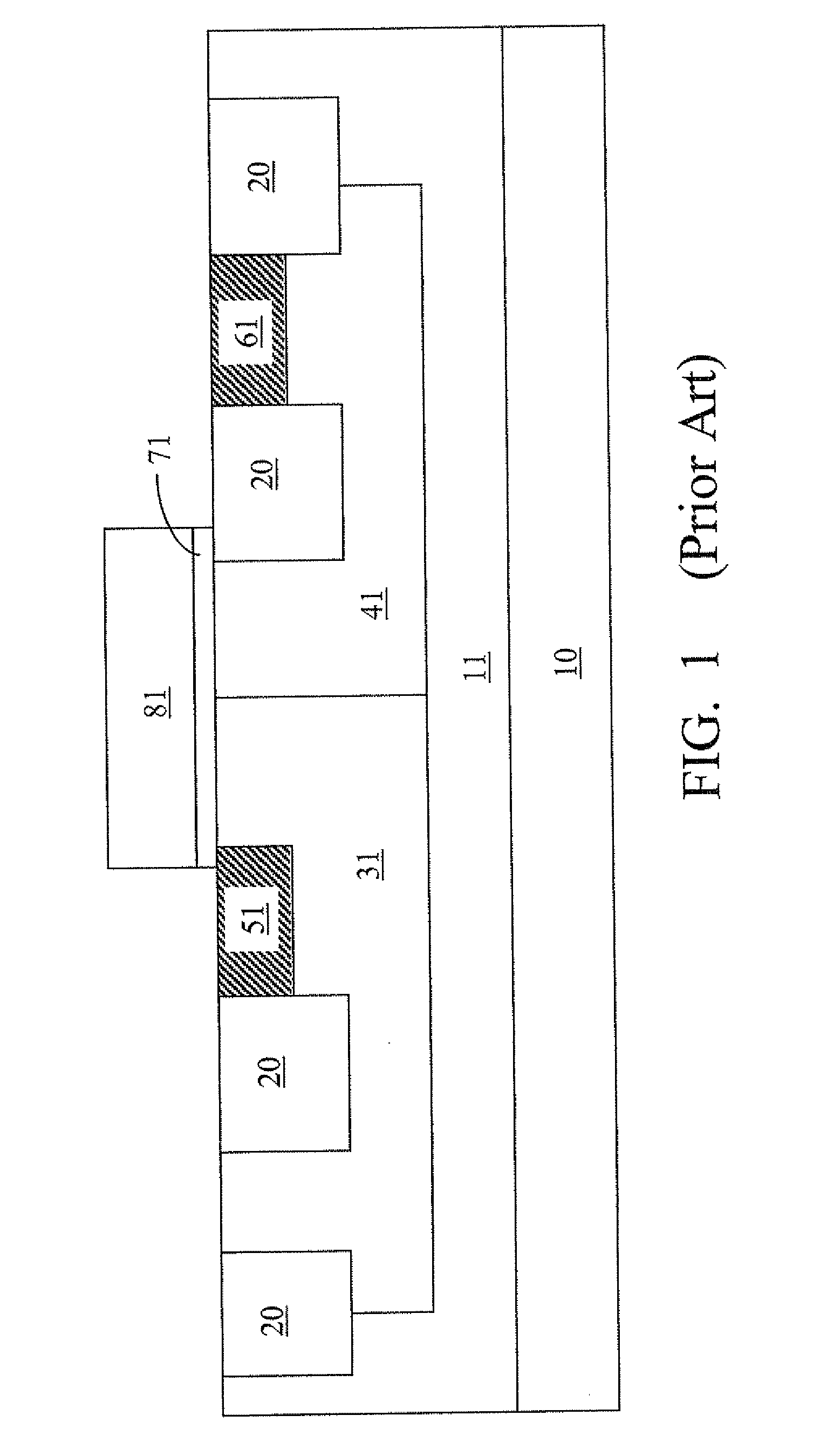
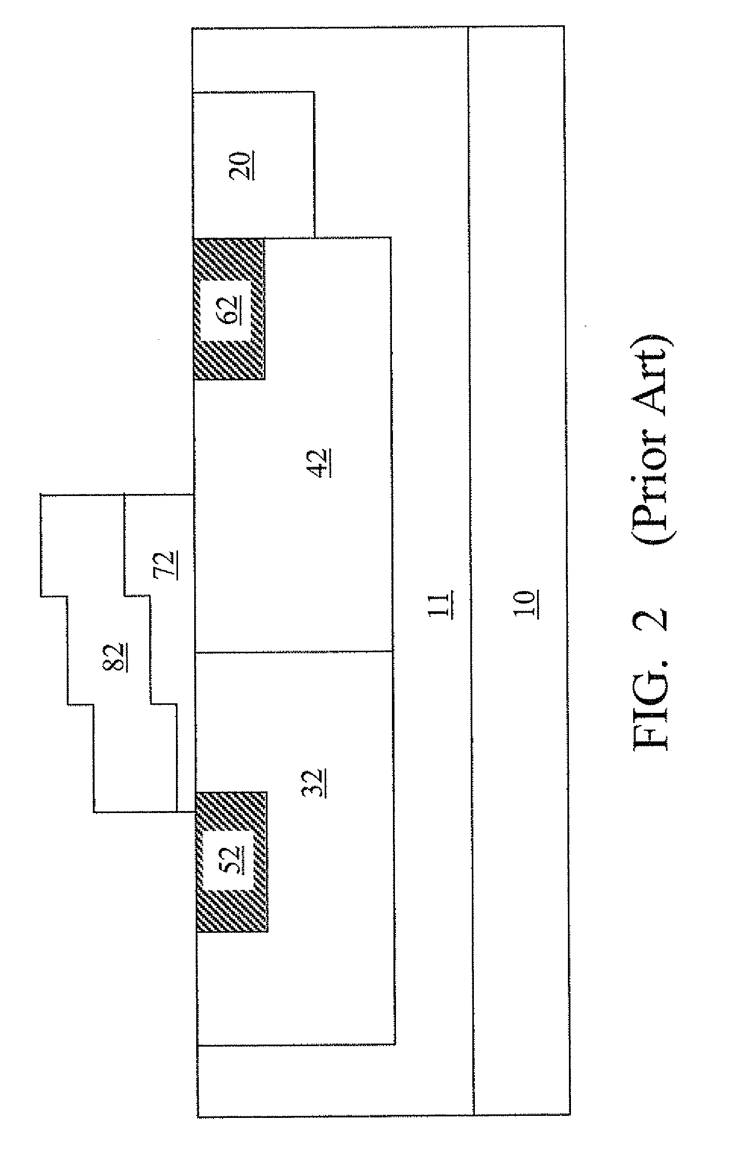
first embodiment
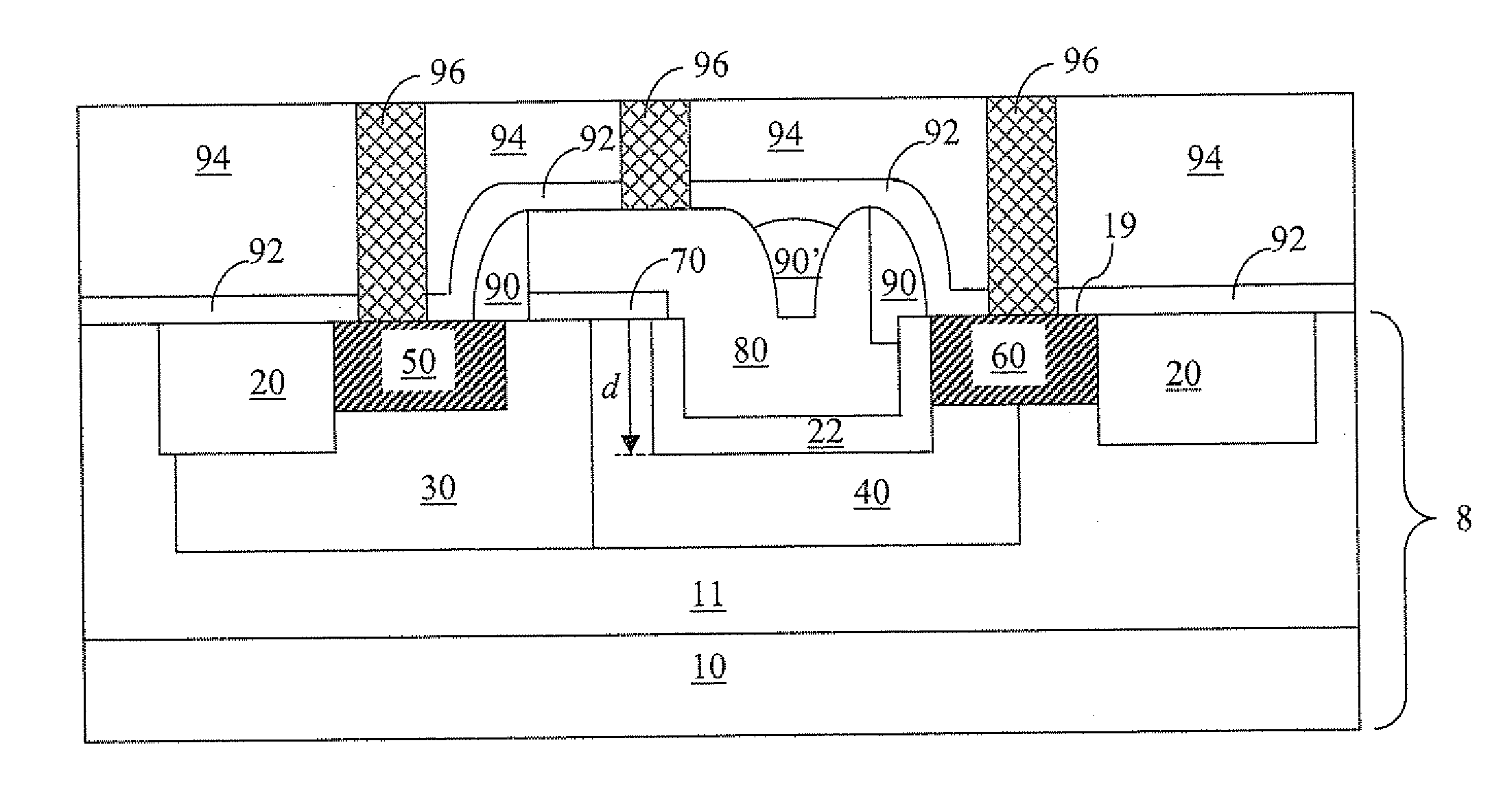
[0082]Referring to FIG. 3, a first exemplary structure according to the present invention comprises a semiconductor substrate 8 containing a substrate layer 10, a tub region 11, a pad layer 12, and a masking layer 14. The substrate layer 10 comprises a silicon containing material such as silicon, a silicon germanium alloy, a silicon carbon alloy, or a silicon germanium carbon alloy. The substrate layer 10 may have a p-type doping or an n-type doping at a typical dopant concentration from about 1.0×10¹⁴ / cm3 to about 1.0×10¹⁶ / cm3. The doping type of the substrate layer 10 is herein referred to as a first conductivity type. The tub region 11 has a second conductivity type, which is opposite to the first. The tub region 11 has a dopant concentration in the range from about 1.0×10¹⁵ / cm3 to about 1.0×10¹⁷ / cm3, although lesser and greater dopant concentrations are also contemplated herein. The tub region 11 may be formed by ion implantation (not shown), which may be followed by an epitaxia...
second embodiment
[0098]Referring to FIG. 14, a second exemplary semiconductor structure according to the present invention is derived from the first exemplary semiconductor structure of FIG. 4 by removing the first photoresist 17 and forming a first dielectric material layer 20P on the exposed surfaces of the shallow trench 18 and the at least another shallow trench 18′. The first dielectric material layer 20P comprises a dielectric material such as a dielectric oxide or a dielectric nitride. For example, the first dielectric material layer 20P may comprise silicon oxide or silicon nitride deposited by chemical vapor deposition (CVD) such as high density plasma chemical vapor deposition (HDPCVD) or low pressure chemical vapor deposition (LPCVD). The first dielectric material layer 20P contains a bottom dielectric portion 20B vertically abutting the trench bottom surface and a sidewall dielectric portion 20S laterally abutting the at least one trench sidewall below the substrate top surface 19. The s...
third embodiment
[0112]Referring to FIG. 25, a third exemplary semiconductor structure according to the present invention is derived from the second exemplary semiconductor structure of FIG. 15 by planarizing, for example, by chemical mechanical polishing (CMP), the conductive material layer 23 to a level that is substantially flush with top surfaces of the first dielectric material layer 20P. A block level photoresist 27 is applied and lithographically patterned to cover the shallow trench 18, while exposing the at least another shallow trench 18′.
[0113]A reactive ion etch or a wet etch may be employed to remove the conductive material layer 23 within the at least another shallow trench 18′, while the portion of the conductive material layer 23 within the shallow trench 8 is protected by the block level photoresist 27. The block level photoresist 27 is subsequently removed.
[0114]Referring to FIG. 26, a second dielectric material layer (not shown) is formed on the first dielectric material layer 20P...
PUM
 Abstract
Description
Claims
Application Information