
Method for manufacturing microcrystalline semiconductor film, thin film transistor having microcrystalline semiconductor film, and photoelectric conversion device having microcrystalline semiconductor film

Inactive Publication Date: 2009-06-04
SEMICON ENERGY LAB CO LTD
View PDF51 Cites 24 Cited by
  • Summary
  • Abstract
  • Description
  • Claims
  • Application Information

AI Technical Summary

Benefits of technology

[0008]A thin film transistor including a polycrystalline semiconductor film has advantages that the mobility thereof is two or more orders of magnitude higher than that of a thin film transistor including an amorphous semiconductor film, and that a pixel portion and a peripheral driver circuit of a semiconductor display device can be formed over one substrate. However, the thin film transistor including a polycrystalline semiconductor film requires a more complicated process than the thin film transistor including an amorphous semiconductor film because of crystallization of the semiconductor film. Thus, there are problems such as reduction in yield and increase in cost.

Problems solved by technology

However, the thin film transistor including a polycrystalline semiconductor film requires a more complicated process than the thin film transistor including an amorphous semiconductor film because of crystallization of the semiconductor film.
Thus, there are problems such as reduction in yield and increase in cost.
Furthermore, in the case where a microcrystalline semiconductor film is formed over a different material, crystallinity of the microcrystalline semiconductor film is low at an interface.
Thus, an inverted staggered thin film transistor including the microcrystalline semiconductor film has a problem in that the crystallinity of an interface region between a gate insulating film and the microcrystalline semiconductor film is low.
In addition, a photoelectric conversion device has a problem in that the crystallinity of an interface between an electrode and the microcrystalline semiconductor film is low.

Method used


Image

  • Method for manufacturing microcrystalline semiconductor film, thin film transistor having microcrystalline semiconductor film, and photoelectric conversion device having microcrystalline semiconductor film
  • Method for manufacturing microcrystalline semiconductor film, thin film transistor having microcrystalline semiconductor film, and photoelectric conversion device having microcrystalline semiconductor film
  • Method for manufacturing microcrystalline semiconductor film, thin film transistor having microcrystalline semiconductor film, and photoelectric conversion device having microcrystalline semiconductor film

Examples


embodiment mode 1

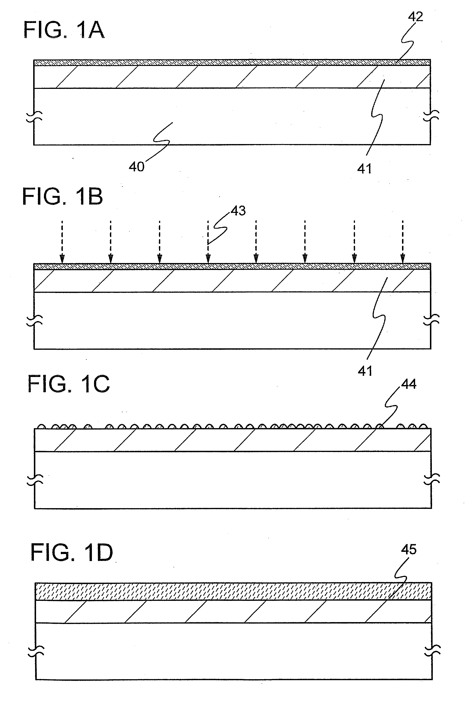
[0062]Here, a method for manufacturing a microcrystalline semiconductor film which has high crystallinity at an interface with a base film and has high adhesion between adjacent crystal grains, namely, a microcrystalline semiconductor film which has fewer defects is described with reference to FIGS. 1A to 1D.

[0063]As illustrated in FIG. 1A, a base film 41 is formed over a substrate 40 so that a semiconductor film 42 is formed over the base film 41.

[0064]As the substrate 40, a plastic substrate having heat resistance that can withstand a processing temperature of the manufacturing process or the like can be used in addition to a non-alkaline glass substrate manufactured by a fusion method or a float method such as a substrate of a barium borosilicate glass, an aluminoborosilicate glass, or an aluminosilicate glass, or a ceramic substrate. Alternatively, a metal substrate such as a stainless steel alloy substrate, which is provided with an insulating film over the surface, may also be...

embodiment mode 2

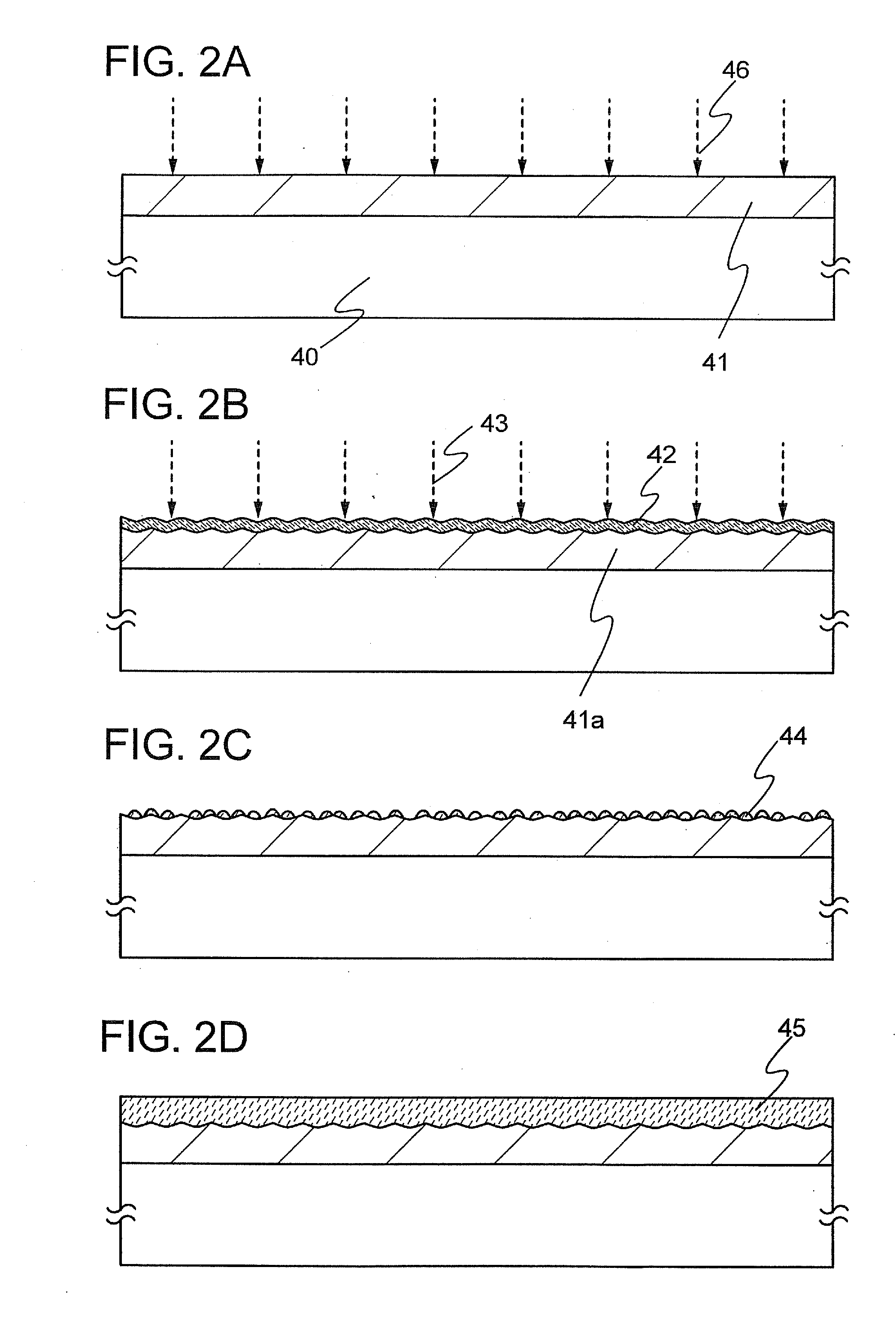
[0084]This embodiment mode describes a process for forming a microcrystalline semiconductor film which has high crystallinity in the entire film and at an interface with a base film with reference to FIGS. 2A to 2D, as in Embodiment Mode 1.

[0085]As illustrate in FIG. 2A, the base film 41 is formed over the substrate 40.

[0086]Next, the surface of the base film 41 is exposed to plasma 46, whereby a base film 41a having an uneven surface with projections and depressions is formed as illustrated in FIG. 2B. Each of the projections and depressions may have a wavelike shape with a gentle curve to form the uneven shape. Alternatively, the projections may have a sharp needle-like shape and the depressions may have a gently curved shape. With small spaces between the projections and depressions, crystal nuclei can be formed at high density later, which is preferable.

[0087]The base film 41 is exposed to the plasma 46 which makes the surface of the base film 41 uneven. Such plasma 46 is genera...

embodiment mode 3

[0093]This embodiment mode describes a method for manufacturing a microcrystalline semiconductor film which has high crystallinity at an interface with a base film and high adhesion between adjacent crystal grains, namely, a microcrystalline semiconductor film which has fewer defects, with reference to FIGS. 3A to 3D.

[0094]As illustrated in FIG. 3A, the base film 41 is formed over the substrate 40, and then the semiconductor film 47 is formed over the base film 41.

[0095]Here, as the semiconductor film 47, a semiconductor film including an impurity element which serves as a donor is formed. The semiconductor film including an impurity element which serves as a donor is formed by a plasma CVD method or a sputtering method. As an impurity element which serves as a donor, phosphorus, arsenic, or antimony is used. Further, as a semiconductor film, an amorphous semiconductor film or a microcrystalline semiconductor film is formed. Furthermore, as an amorphous semiconductor film or a micro...


PUM


Abstract

A method for forming a microcrystalline semiconductor film over a base formed of a different material, which has high crystallinity in the entire film and at an interface with the base, is proposed. Further, a method for manufacturing a thin film transistor including a microcrystalline semiconductor film with high crystallinity is proposed. Furthermore, a method for manufacturing a photoelectric conversion device including a microcrystalline semiconductor film with high crystallinity is proposed. By forming crystal nuclei with high density and high crystallinity over a base film and then growing crystals in a semiconductor from the crystal nuclei, a microcrystalline semiconductor film which has high crystallinity at an interface with the base film, which has high crystallinity in crystal grains, and which has high adhesion between the adjacent crystal grains is formed.

Description

BACKGROUND OF THE INVENTION[0001]1. Field of the Invention[0002]The present invention relates to a method for manufacturing a microcrystalline semiconductor film, a method for manufacturing a thin film transistor having the microcrystalline semiconductor film, and a method for manufacturing a photoelectric conversion device having at least one pair of semiconductor junctions in the microcrystalline semiconductor film.[0003]2. Description of the Related Art[0004]In recent years, technology for forming thin film transistors using a thin semiconductor film (with a thickness of from several tens of nanometers to several hundred nanometers, approximately) formed over a substrate having an insulating surface has been attracting attention. Thin film transistors are applied to a wide range of electronic devices such as ICs or electro-optical devices, and prompt development of thin film transistors that are to be used as switching elements in image display devices, in particular, is being pu...

Claims


Application Information

Patent Timeline
IPC IPC(8): H01L21/20
CPCH01L21/0237H01L21/02436H01L21/02595H01L21/0262H01L27/1214H01L29/04Y02E10/548H01L29/4908H01L29/78696H01L31/03685H01L31/1824Y02E10/545H01L29/458H01L27/1288H01L27/127Y02P70/50
Inventor JINBO, YASUHIROMIYAIRI, HIDEKAZUDAIRIKI, KOJI
Owner SEMICON ENERGY LAB CO LTD
Features
  • Generate Ideas
  • Intellectual Property
  • Life Sciences
  • Materials
  • Tech Scout
  • Unparalleled Data Quality
  • Higher Quality Content
  • 60% Fewer Hallucinations
Learn More