Nanoscale metal paste for interconnect and method of use

Active Publication Date: 2009-06-25
VIRGINIA TECH INTPROP INC
View PDF9 Cites 68 Cited by
  • Summary
  • Abstract
  • Description
  • Claims
  • Application Information

AI Technical Summary

Benefits of technology

[0013]The nanosilver paste of this invention may also be formed into nanosilver preforms for easy handling and application. Nanosilver performs are formed by drying an amount of nanosilver

Problems solved by technology

However, high applied pressure is not the norm in the packaging industry and could pose serious complications to the attachment/interconnection process, which in turn could lead to more failures (e.g., cracked die) and h

Method used


Image

  • Nanoscale metal paste for interconnect and method of use
  • Nanoscale metal paste for interconnect and method of use
  • Nanoscale metal paste for interconnect and method of use

Examples


example 1

[0060]Method for Regulating the Densification of Silver by Binder System Composition

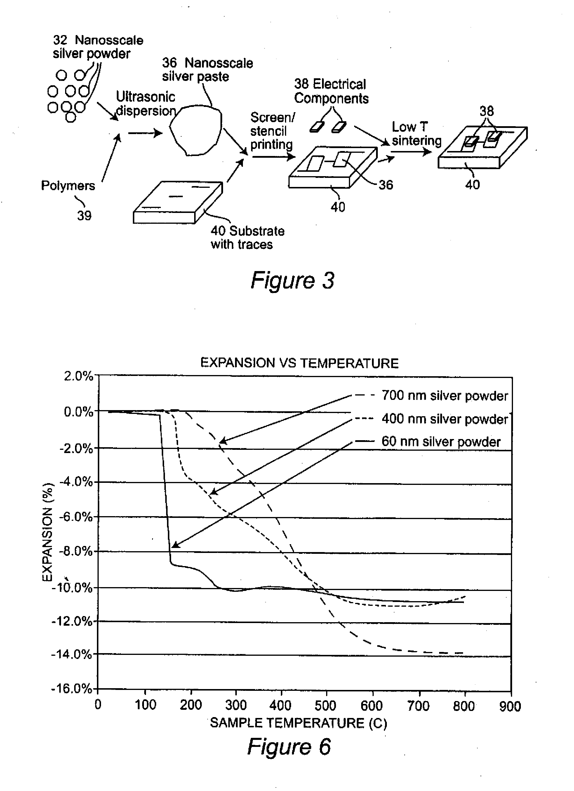
[0061]Regulation of the densification temperature / rate of the metal particles in the paste of this invention can be achieved by adjusting the type of components that go into the binder system. In particular, it is possible to increase or reduce the firing temperature for any given particle size of the silver (or other metal or metal alloy). For example, if it is desired to increase the effective onset of densification of, for example, a nanosilver paste as discussed above, this can be achieved by substituting the binder system components with alternatives that burn out at higher temperatures to closely match the desired or target peak processing temperature (e.g., the binder system might be chosen to vaporize or otherwise decompose at a temperature that is the same as or slightly below (e.g., within 50° C. or 30° C. or 10° C.) the sintering temperature for the metal or metal alloy particles. This has...

example 2

[0063]Time-Temperature Heating Profile for Applying Nanosilver Paste Without Pressure

[0064]Electric devices were bonded onto a direct bonded copper (DBC) substrate as shown schematically in FIGS. 8a and 8b.

[0065]Step I—FIG. 8a.

Between 50-100 micron (2-4 mil.) of nanosilver paste was stenciled on a DBC substrate plated with nickel and silver. The nanosilver paste was dried using the following temperature profile:[0066]0-10 min.—50° C.[0067]10-15 min.—75° C.[0068]15-20 min.—100° C.[0069]20-30 min.—125° C.[0070]30-40 min.—210° C.

[0071]The substrate and nanosilver paste were then allowed to cool to room temperature.

[0072]Step II—FIG. 8b.

[0073]Another 5-15 micro layer of nanosilver paste was stenciled on top of the dried paste layer. Silicon dummy devices were attached with a smearing motion. The die-attachment was then sintered according to the following temperature profile:[0074]0-1.5 min.—50° C.[0075]1.5-3.0 min.—75° C.[0076]3.0-4.5 min.—100° C.[0077]4.5-6.0 min.—125° C.[0078]6.0-1...

example 3

[0080]Time-Temperature Heating Profile for Applying Nanosilver Paste With Pressure

[0081]Electric devices were bonded onto a DBC substrate as shown schematically in FIGS. 9a and 9b.

[0082]Step I—FIG. 9a.

[0083]Between 50-100 micron (2-4 mil.) of nanosilver paste was stenciled on a DBC substrate plated with nickel and silver. The nanosilver paste was dried using the following temperature profile:[0084]0-20 min.—50° C.[0085]20-25 min.—75° C.[0086]25-30 min.—100° C.[0087]30-50 min.—125° C.[0088]50-60 min.—150° C.

[0089]The substrate and nanosilver paste were then allowed to cool to room temperature.

[0090]Step II—FIG. 9b.

[0091]Electronic devices were mounted onto the dried nanosilver film. Between 3-5 MPa external pressure was applied and the die-attachment was sintered according to the following temperature profile to form a conductive joint:[0092]0-1.5 min.—50° C.[0093]1.5-3.0 min.—75° C.[0094]3.0-4.5 min.—100° C.[0095]4.5-6.0 min.—125° C.[0096]6.0-16 min.—250° C.

[0097]The die-attachme...


PUM

PropertyMeasurementUnit
Temperatureaaaaaaaaaa
Pressureaaaaaaaaaa

Abstract

A paste including metal or metal alloy particles (which are preferably silver or silver alloy), a dispersant material, and a binder is used to form an electrical, mechanical or thermal interconnect between a device and a substrate. By using nanoscale particles (i.e., those which are less than 500 nm in size and most preferably less than 100 nm in size), the metal or metal alloy particles can be sintered at a low temperature to form a metal or metal alloy layer which is desired to allow good electrical, thermal and mechanical bonding, yet the metal or metal alloy layer can enable usage at a high temperature such as would be desired for SiC, GaN, or diamond (e.g., wide bandgap devices). Furthermore, significant application of pressure to form the densified layers is not required, as would be the case with micrometer sized particles. In addition, the binder can be varied so as to insulate the metal particles until a desired sintering temperature is reached; thereby permitting fast and complete sintering to be achieved.

Description

STATEMENT OF PRIORITY[0001]This application is a continuation-in-part of U.S. patent application Ser. No. 10 / 589,399, filed on Aug. 14, 2006, published as U.S. Patent Application Publication No. 2007 / 0183920, which claims priority to the PCT Application No. PCT / US2005 / 004567, filed Feb. 14, 2005, which in turn claims priority to the U.S. Provisional Application Ser. No. 60 / 545,139, filed Feb. 18, 2004. The disclosure of these applications is hereby incorporated by reference herein.BACKGROUND OF THE INVENTION[0002]1. Field of the Invention[0003]The present invention generally relates to materials used for interconnecting electronic devices and, particularly, devices which either generate high temperatures during use or devices which are used in high temperature applications. Furthermore, the invention is generally related to a fabrication method which reduces or eliminates the need for high pressure application during fabrication of an interconnection, such as during die attach.[0004...

Claims


Application Information

Patent Timeline
IPC IPC(8): B05D3/02B22F7/02B22F1/10B22F1/103
CPCB22F1/0059B22F7/064B22F2001/0066B22F2998/00B22F2998/10H01L24/29H01L24/83H01L2224/29339H01L2224/83801H01L2224/8384H01L2924/01005H01L2924/01011H01L2924/01013H01L2924/01029H01L2924/01046H01L2924/01047H01L2924/01049H01L2924/0105H01L2924/01074H01L2924/01078H01L2924/01079H01L2924/01082H01L2924/01322H01L2924/14H01L2924/19041H01L2924/3025H05K3/321H05K2201/0257H05K2203/1131H01L24/75H01L2224/2919H01L2224/83439H01L2224/83444H01L2924/01006H01L2924/01019H01L2924/01023H01L2924/01033H01L2924/014H01L2924/0665H01L2224/29101H01L2924/0132H01L2224/29082H01L2224/29111H01L2224/83192H01L2924/12041H01L2224/29139H01L2224/83101B22F1/0018B22F3/1021B22F3/15H01L2924/00H01L2924/3512H01L2924/00014H01L2924/00015H01L2924/203H05K3/341H05K2203/1126H01L2224/83204B22F1/103B22F1/10H01L2924/0002
Inventor LU, GUO-QUANLEI, GUANGYINCALATA, JESUS N.
Owner VIRGINIA TECH INTPROP INC
Why Eureka
Try Eureka