Method for manufacturing soi substrate

Inactive Publication Date: 2009-07-02
SEMICON ENERGY LAB CO LTD
View PDF15 Cites 38 Cited by
  • Summary
  • Abstract
  • Description
  • Claims
  • Application Information

AI Technical Summary

Benefits of technology

[0021]According to the present invention, adhesion between a semiconductor substrate and a base substrate can be improved and occurrence of defective bondin

Problems solved by technology

However, in the case of using a base substrate which has an uneven surface, defective bonding occurs when the base substrate and a single crystal semiconductor substrate are bonded to each other.
As a result, a region (defect) where a single crystal silicon film is not formed over the base substrate is caused.
In the case where a semiconductor element such as a transistor is formed using an SOI substrate which has such a defect, an operation defect may occur.
In particular, it is thought that such a proble

Method used


Image

  • Method for manufacturing soi substrate
  • Method for manufacturing soi substrate
  • Method for manufacturing soi substrate

Examples


embodiment mode 1

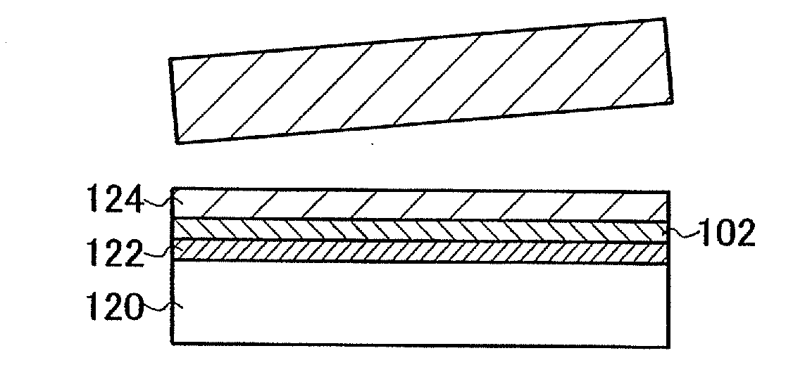
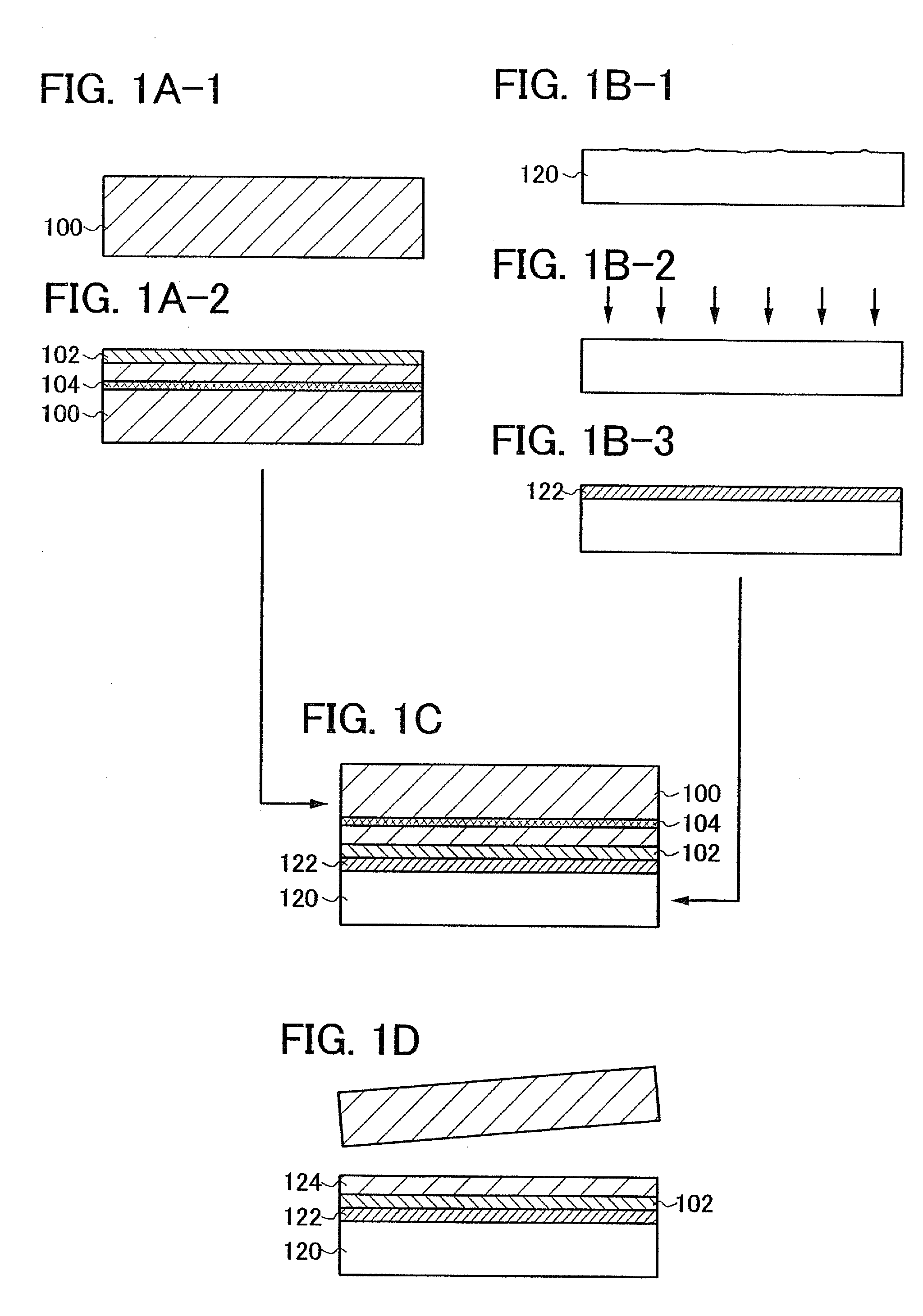
[0058]This embodiment mode describes an example of a method for manufacturing an SOI substrate of the present invention with reference to drawings. Specifically, a method is described in which an insulating film based on silicon is formed on a semiconductor substrate side, an insulating film containing aluminum is formed on a base substrate side, and the semiconductor substrate and the base substrate are bonded to each other.

[0059]First, a semiconductor substrate 100 is prepared (see FIG. 1A-1).

[0060]As the semiconductor substrate 100, a commercially available semiconductor substrate can be used. For example, a single crystal silicon substrate, a single crystal germanium substrate, and a compound semiconductor substrate of gallium arsenide, indium phosphide, or the like can be used. Typical examples of commercially available silicon substrates are circular silicon substrates which are 5 inches (125 mm) in diameter, 6 inches (150 mm) in diameter, 8 inches (200 mm) in diameter, and 12...

embodiment mode 2

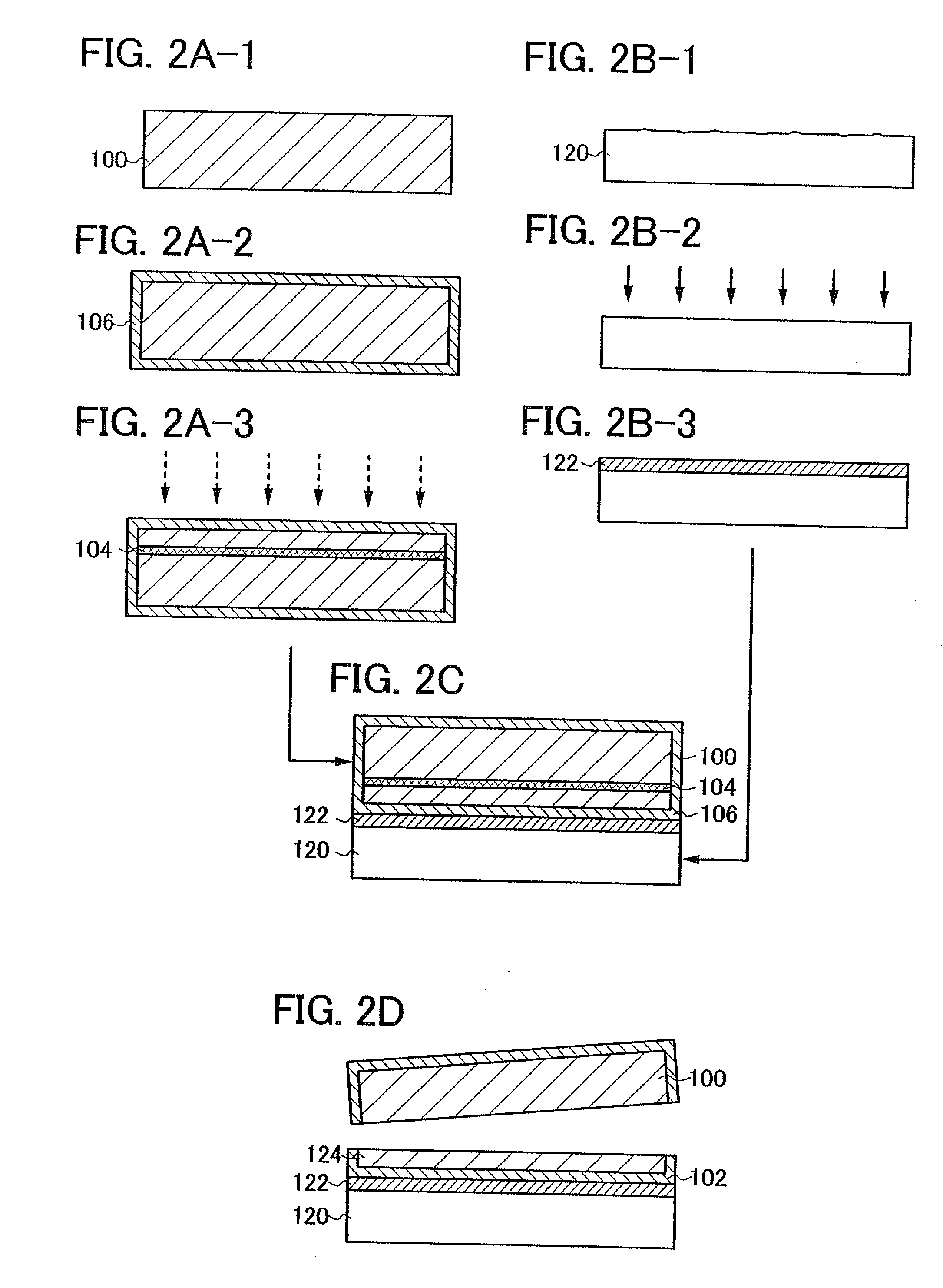
[0109]This embodiment mode describes a method for manufacturing an SOI substrate which is different from that in the above-described embodiment mode with reference to drawings. Specifically, a case is described in which an insulating film based on silicon is formed over a semiconductor substrate through thermal oxidation treatment.

[0110]First, the semiconductor substrate 100 is prepared (see FIG. 2A-1). Note that it is preferable that the semiconductor substrate 100 be cleaned using a sulfuric acid / hydrogen peroxide mixture (SPM), an ammonium hydroxide / hydrogen peroxide mixture (APM), a hydrochloric acid / hydrogen peroxide mixture (HPM), dilute hydrogen fluoride (DHF), or the like as appropriate.

[0111]Next, thermal oxidation treatment is performed on the semiconductor substrate 100 in order to form an oxide film 106 (see FIG. 2A-2).

[0112]Thermal oxidation treatment may be performed by dry oxidation; however, it is preferable that thermal oxidation treatment be performed in an oxidati...

embodiment mode 3

[0129]This embodiment mode describes a method for manufacturing an SOI substrate in which a semiconductor substrate is repeatedly used (reused) with reference to drawings. Further, this embodiment mode describes a case in which the semiconductor substrate 100 which has rounded corners (end portions) (with edge roll-off (ERO)) is used.

[0130]First, a process A is performed in which the semiconductor substrate 100 (single crystal semiconductor substrate in this embodiment mode) which is provided with the first insulating film 102 over the surface and in which the separation layer 104 is formed at a predetermined depth from the surface is prepared (see FIG. 3A and FIG. 4A). In the process A, cleaning of the semiconductor substrate 100, formation of the first insulating film 102, addition of ions to the semiconductor substrate 100, surface treatment on the first insulating film 102, and the like are performed. The detailed description of these processes is omitted because the method show...


PUM


Abstract

A single crystal semiconductor substrate and a base substrate are prepared; a first insulating film is formed over the single crystal semiconductor substrate; a separation layer is formed by introducing ions at a predetermined depth through a surface of the single crystal semiconductor substrate; plasma treatment is performed on the base substrate so as to planarize a surface of the base substrate; a second insulating film is formed over the planarized base substrate; a surface of the first insulating film is bonded to a surface of the second insulating film by making the surface of the single crystal semiconductor substrate and the surface of the base substrate face each other; and a single crystal semiconductor film is provided over the base substrate with the second insulating film and the first insulating film interposed therebetween by performing separation at the separation layer.

Description

BACKGROUND OF THE INVENTION[0001]1. Field of the Invention[0002]The present invention relates to a silicon-on-insulator (SOI) substrate, a manufacturing method thereof, a semiconductor device using the SOI substrate, and a manufacturing method thereof.[0003]2. Description of the Related Art[0004]In recent years, integrated circuits using a silicon-on-insulator (SOI) substrate where a thin single crystal semiconductor film is present over an insulating surface, instead of using a bulk silicon wafer, have been developed. Because parasitic capacitance between a drain of a transistor and a substrate is reduced by use of an SOI substrate, SOI substrates are attracting attention as substrates which improve performance of semiconductor integrated circuits.[0005]One of known methods for manufacturing SOI substrates is a Smart Cut (registered trademark) method. A summary of a method for manufacturing an SOI substrate by a Smart Cut method is described below. First, by implantation of hydroge...

Claims


Application Information

Patent Timeline
IPC IPC(8): H01L21/762
CPCH01L21/76254H01L21/20
Inventor ENDO, YUTAYAMAZAKI, SHUNPEI
Owner SEMICON ENERGY LAB CO LTD
Why Eureka
Try Eureka