Method For Fabricating Capacitor Structures Using The First Contact Metal

a capacitor and metal technology, applied in the field of metal capacitor/gate electrode structure fabrication, can solve the problems of adding significant complexity and undesirable chau to the conventional cmos (single-polysilicon) process, and achieve the effect of high capacitance and small layout area

Active Publication Date: 2009-09-24
TOWER SEMICONDUCTOR
View PDF11 Cites 17 Cited by
  • Summary
  • Abstract
  • Description
  • Claims
  • Application Information

AI Technical Summary

Benefits of technology

[0005]Accordingly the present invention provides improved methods for fabricating metal electrodes over dielectric materials, wherein such methods can be robustly integrated into a conventional CMOS process flow without changing the properties of the other devices fabricated on the same wafer. The metal electrodes fabricated in accordance with the present invention may be used as upper capacitor electrodes, wherein the lower capacitor electrodes are formed by (salicided or non-salicided) polysilicon layers or (salicided or non-salicided) silicon active areas. Capacitors fabricated in this manner exhibit a small layout area and a high capacitance. The metal electrodes fabricated in accordance with the present invention may alternately be used for other applications, such as forming gate electrodes of high-voltage silicon-on-insulator (SOI) transistors, or control gates of electrically erasable programmable read only memory (EEPROM) cells.

Problems solved by technology

However, Chau undesirably adds significant complexity to a conventional CMOS (single-polysilicon) process because three (non-standard) metal layers must be deposited prior to depositing the polysilicon layer.
However, Sung et al. undesirably requires the addition of the following steps to a conventional CMOS process: a control gate mask formation, control gate etch, oxidation treatment, Al2O3 deposition, barrier metal (TiN) deposition, tungsten (W) fill, chemical-mechanical polishing (CMP) and post ALD anneal.

Method used


Image

  • Method For Fabricating Capacitor Structures Using The First Contact Metal
  • Method For Fabricating Capacitor Structures Using The First Contact Metal
  • Method For Fabricating Capacitor Structures Using The First Contact Metal

Examples


Embodiment Construction

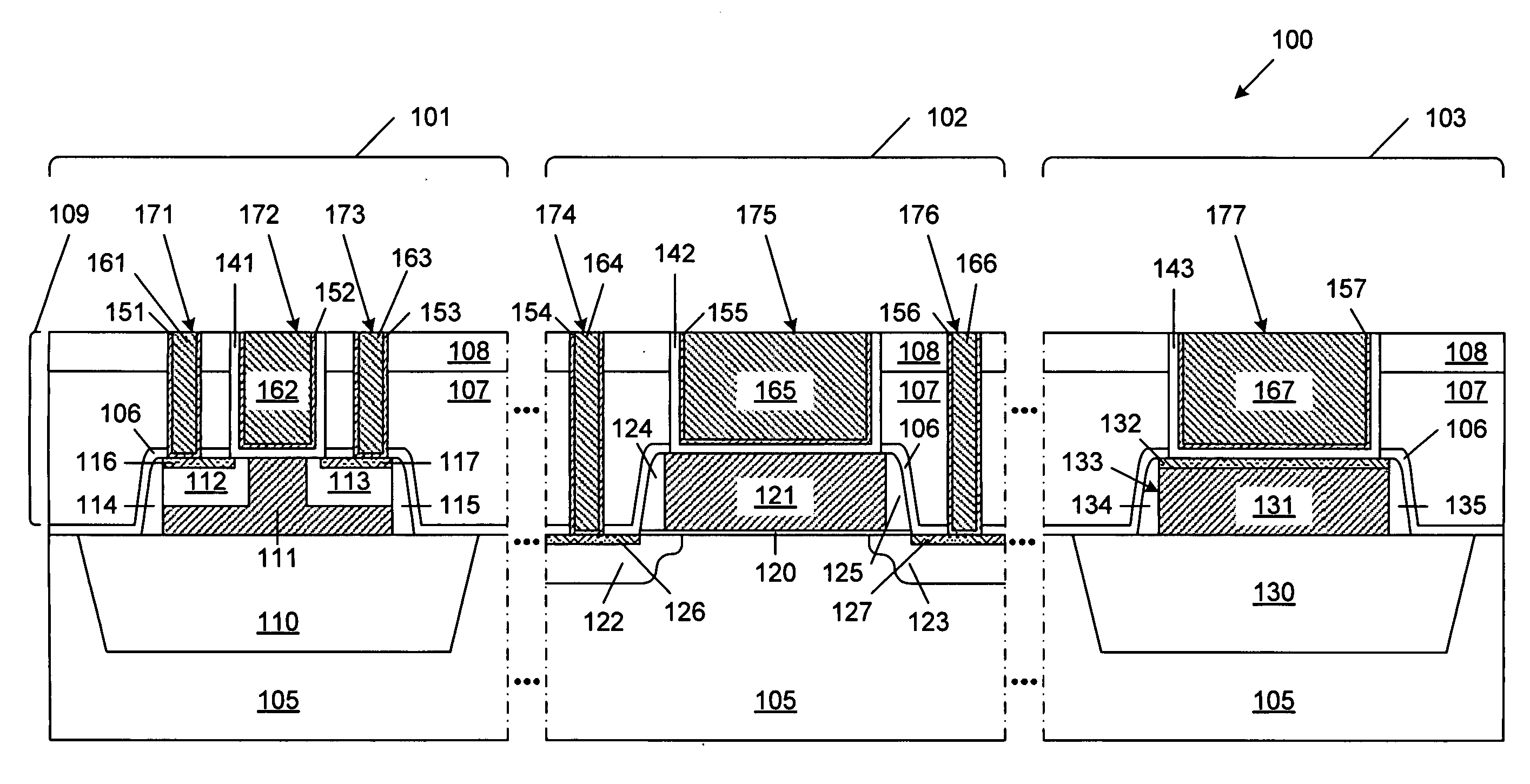
[0016]FIG. 1 is a cross-sectional view of a semiconductor structure 100 in accordance with one embodiment of the present invention. Semiconductor structure 100 includes three semiconductor devices 101, 102 and 103, which may fabricated on the same semiconductor substrate 105. Semiconductor devices 101, 102 and 103 will now be briefly described.

[0017]Semiconductor device 101 is a high-voltage (e.g., 25 to 40 Volt) silicon-on-insulator (SOI) transistor, which includes shallow trench isolation (STI) region 110, polysilicon body region 111, source / drain regions 112-113, dielectric sidewall spacers 114-115, metal salicide source / drain contact regions 116-117, dielectric barrier layer 106, pre-metal dielectric structure 109 (which includes pre-metal dielectric layer 107 and pre-metal dielectric cap 108), gate dielectric layer 141, source / drain contact plug 171 (which includes composite metal barrier region 151 and metal contact structure 161), source / drain contact 173 (which includes comp...


PUM


Abstract

A capacitor structure is fabricated with only slight modifications to a conventional single-poly CMOS process. After front-end processing is completed, grooves are etched through the pre-metal dielectric layer to expose polysilicon structures, which may be salicided or non-salicided. A dielectric layer is formed over the exposed polysilicon structures. A conventional contact process module is then used to form contact openings through the pre-metal dielectric layer. The mask used to form the contact openings is then removed, and conventional contact metal deposition steps are performed, thereby simultaneously filling the contact openings and the grooves with the contact (electrode) metal stack. A planarization step removes the upper portion of the metal stack, thereby leaving metal contacts in the contact openings, and metal electrodes in the grooves. The metal electrodes may form, for example, transistor gates, EEPROM control gates or capacitor plates.

Description

FIELD OF THE INVENTION[0001]The present invention relates to improved methods for fabricating a metal capacitor / gate electrode structure.RELATED ART[0002]Metal gate electrodes have been used in conventional CMOS transistor applications. For example, U.S. Pat. No. 6,998,686 to Chau describes a multi-layer material stack for CMOS application. However, Chau undesirably adds significant complexity to a conventional CMOS (single-polysilicon) process because three (non-standard) metal layers must be deposited prior to depositing the polysilicon layer.[0003]Metal electrodes have also been used to implement the control gate of an EEPROM structure, as set forth by H. C. Sung et al., “Novel Single Poly EEPROM with Damascene Control Gate Structure”, IEEE Electron Device Letter 2005, pp. 770. However, Sung et al. undesirably requires the addition of the following steps to a conventional CMOS process: a control gate mask formation, control gate etch, oxidation treatment, Al2O3 deposition, barrie...

Claims


Application Information

Patent Timeline
Patent Type & Authority Applications(United States)
IPC IPC(8): H01L21/02H01L21/28
CPCH01L21/28273H01L28/60H01L27/105H01L27/0733H01L29/40114
Inventor ALONI, EFRAIMROIZIN, YAKOVHELMAN, ALEXEYLISIANSKY, MICHAELFENIGSTEIN, AMOSBUCHBINDER, MYRIAM
Owner TOWER SEMICONDUCTOR
Why Eureka
Try Eureka