
Memory cell device having vertical channel and double gate structure

a memory cell and gate structure technology, applied in semiconductor devices, instruments, electrical devices, etc., can solve the problems of high integration, high integration difficulty, and retained limitations, and achieve high integration, high integration, and increase the amount of reading current.

Active Publication Date: 2009-10-01
SEOUL NAT UNIV R&DB FOUND
View PDF9 Cites 6 Cited by
  • Summary
  • Abstract
  • Description
  • Claims
  • Application Information

AI Technical Summary

Benefits of technology

[0011]To solve the problems, the present invention is directed to a nonvolatile memory cell having a vertical channel and a double gate structure by forming a pillar active region having a vertical channel by accumulating a plurality of semiconductor layers. So, there is no need for unnecessary contacts when a nonvolatile memory cell in the present invention is used as a unit cell for any other types of memory array, not to speak of NOR type flash memory array, and it makes it possible to overcome the high integration limitation in the conventional memory devices.
[0012]In addition, another aspect of the present invention is to provide a nonvolatile memory cell having a vertical channel and a double gate structure, which has an insulating layer comprised of two or more dielectric layers on the both sides of a pillar active region. So, the present invention can make to program / erase more effectively and increase the read speed and the amount of sensing current, and it can solve the uniformity problem of a tunnel oxide layer in the conventional planar type memory cell thoroughly.
[0017]The second insulating layer can be the same as the first insulating layer and it can make a fabricating process simpler.
[0018]According to the present invention, even if a memory cell of the present invention can be used as a unit cell for not only NOR type flash memory array but also any other types of memory array, different electrical signal lines are connected respectively to a first semiconductor layer and a second semiconductor layer which are formed in a pillar active region with a predetermined height, and high integration for any type of memory is possible because there is no need for unnecessary contacts.
[0019]By forming a first insulating layer comprising two or more dielectric layers including charge trap layers on both sides of a pillar active region, program / erase can be done effectively, and the read speed and the amount of sensing current can be increased.
[0020]In addition, by controlling the height of a third semiconductor layer as a body region and a channel region, a charge trap layer can be extended and the uniformity problem of a tunnel oxide layer in the conventional planar type memory cell can be overcome thoroughly.

Problems solved by technology

However, unlike a NAND type flash memory, it has a difficulty in high-integration due to the increasing area of a bit line contact and a source line.
However, the way to improve the memory integration by reducing the channel width in the planar type device structure has retained some limitations related with the semiconductor process technology and the device operation.
However, such attempts have the limitation on high integration due to the area of a bit line contact and source line.

Method used


Image

  • Memory cell device having vertical channel and double gate structure
  • Memory cell device having vertical channel and double gate structure
  • Memory cell device having vertical channel and double gate structure

Examples


first embodiment

[First Embodiment]

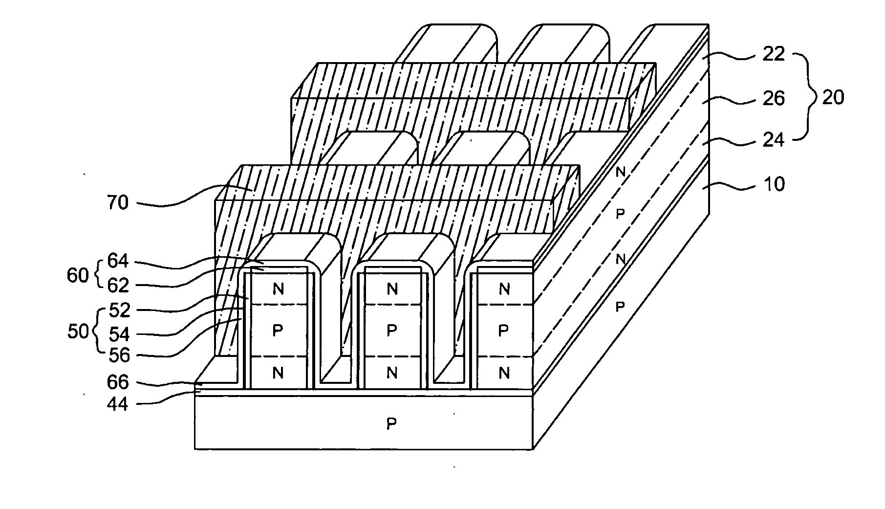
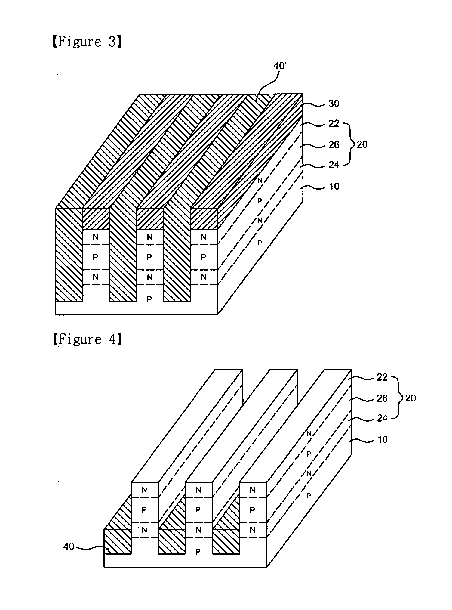
[0031]In the basic structure, a field region 40 is formed with an oxide layer filling a space with a predetermined thickness between neighboring pillar active regions under one side of the second semiconductor layer 24, as shown in FIG. 6.

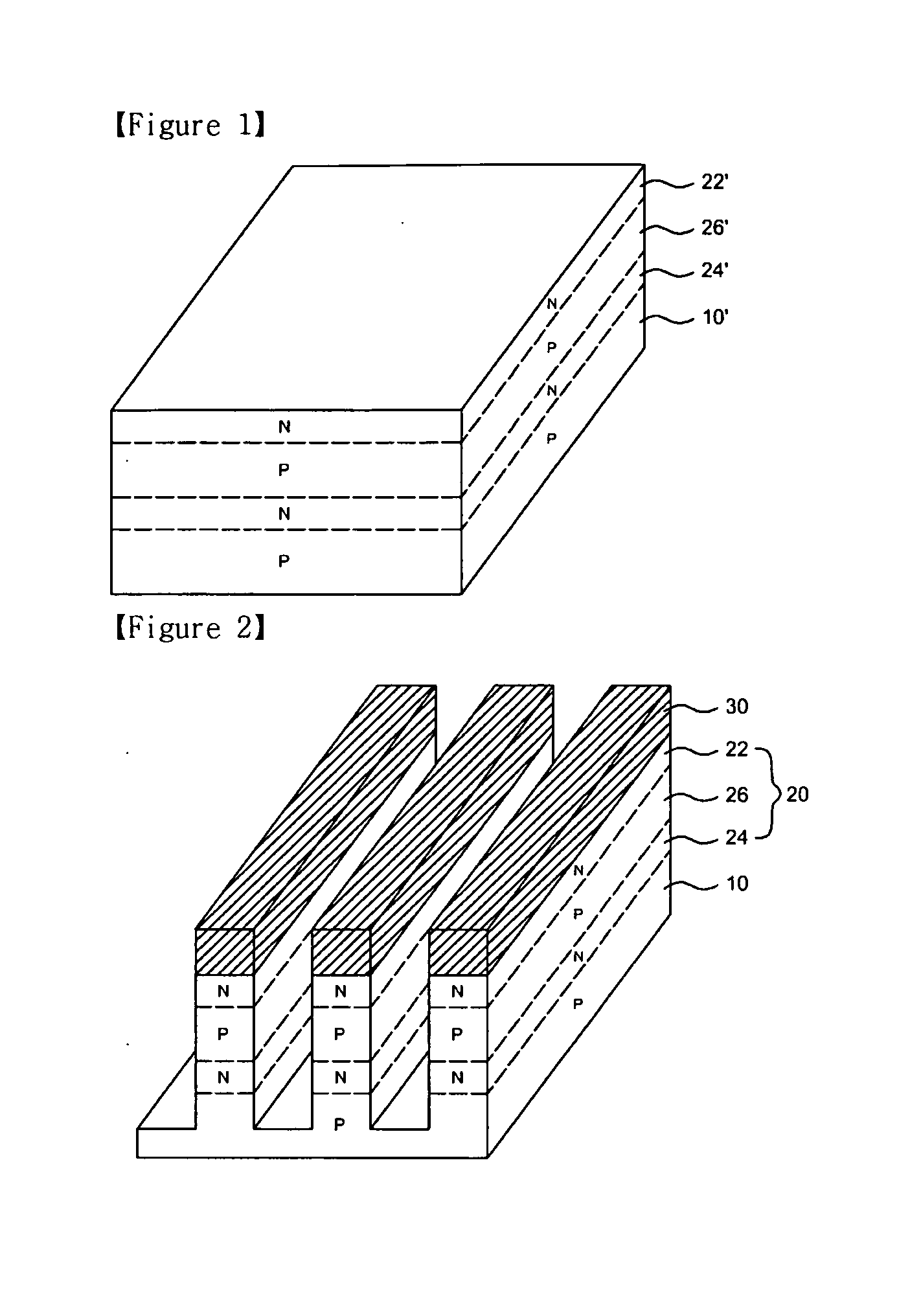
[0032]FIGS. 1 to 6 show the fabricating process according to the first embodiment of the present invention.

[0033]First of all, as shown in FIG. 1, an N-type doping layer 24′ is formed uniformly in the deep site by injecting N-type impurities with proper dose and energy to a P-type semiconductor substrate 10′ to form a second semiconductor layer 24. Then, the same N-type doping layer 22′ is formed uniformly in the shallow site by injecting the same N-type impurities with the same dose but smaller energy to a P-type semiconductor substrate 10′ to form a first semiconductor layer 22. It is more preferable to form a P-type doping layer 26′ for forming a third semiconductor layer 26 by injecting P-type impurities with proper dose and e...

second embodiment

[Second Embodiment]

[0039]A memory cell of the present invention can be embodied by using a SOI substrate, as shown in FIG. 11. In the basic structure, the pillar active region 20 is formed with a silicon layer of a SOI substrate and the field region is a buried oxide layer 42 of a SOI substrate.

[0040]FIGS. 7 to 11 show the fabricating process according to the second embodiment of the present invention.

[0041]The fabricating process for the second embodiment is almost the same as the fabricating process for the first embodiment. Differences between the two fabricating processes are following:

[0042]First, as shown in FIG. 7, NPN doping layers 22′, 24′ and 26′ are formed orderly in the silicon layer of a SOI substrate.

[0043]Then, as shown in FIG. 8, a pillar active region 20 with a predetermined height is formed by using a nitride layer or other material mask 30 and etching silicon. The etching silicon should be done to reveal the buried oxide layer 42. Unlike the first embodiment, ther...

third embodiment

[Third Embodiment]

[0046]A memory cell of the present invention, as shown in FIG. 17, in the basic structure, a field region is formed with a oxide layer 44 formed by an oxidative encroachment on a bulk silicon substrate 10 under the second semiconductor layer 24.

[0047]FIGS. 12 to 17 show the fabricating process according to the third embodiment of the present invention.

[0048]The fabricating process for the third embodiment is almost the same as the fabricating process for the first embodiment. Differences between the two fabricating processes are following:

[0049]First, as shown in FIG. 12, NPN doping layers 22′, 24′ and 26′ are formed orderly onto a P-type bulk substrate. It is preferable for the N-type doping layer 24′ for the second semiconductor layer 24 to be formed slightly thicker than the N-type doping layer 24′ in the first embodiment.

[0050]Then, as shown in FIG. 13, a pillar active region 20 with a predetermined height is formed by forming a nitride layer mask 30 and etchin...


PUM


Abstract

A memory cell device having a vertical channel and a double gate structure is provided. More specifically, a memory cell device having a vertical channel and a double gate structure is characterized by having a pillar active region with a predetermined height, which is including a first semiconductor layer forming a first source / drain region, a second semiconductor layer being placed under the first semiconductor layer with a predetermined distance and forming a second source / drain region, and a third semiconductor layer forming a body region and a channel region between the first semiconductor layer and the second semiconductor layer, and therefore, there is no need for unnecessary contacts when it is used as a unit cell for any type of memory array, not to speak of NOR type flash memory array. And the present invention makes to program / erase more effectively and increase the read speed and the amount of sensing current.

Description

BACKGROUND OF THE INVENTION[0001]1. Field of the Invention[0002]The present invention relates to a nonvolatile memory device, and more specifically to a nonvolatile memory cell structure having a vertical channel and a double gate structure.[0003]2. Description of the Related Art[0004]Currently, a nonvolatile memory device has characteristics to remove and store data electrically, and store data even if electric power supply is unavailable, and therefore, it has been used widely for electronic equipment such as memory cards for music or image data and mobile phones for which constant electric power supply is impossible or electric power supply is stopped intermittently.[0005]While a flash memory device selects one cell structure for one transistor to overcome the integrity limit of EEPROM (Electrically Erasable Programmable Read Only Memory), it makes to input or output data electrically and freely, and the demand for the flash memory device has increased rapidly along with the deve...

Claims


Application Information

Patent Timeline
Patent Type & Authority Applications(United States)
IPC IPC(8): H01L29/792H10B69/00
CPCH01L27/11568H01L27/115H10B43/30H10B69/00H01L29/40117G11C16/0483H10B63/80
Inventor PARK, BYUNG GOOKPARK, II HAN
Owner SEOUL NAT UNIV R&DB FOUND
Learn More