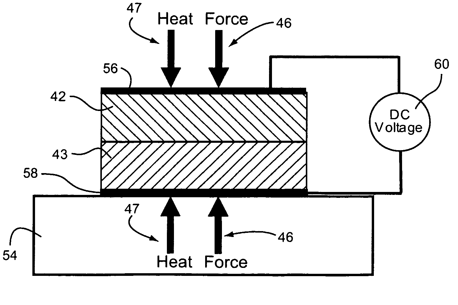
Low-temperature wafer bonding of semiconductor substrates to metal substrates

a technology of metal substrates and wafers, which is applied in the direction of semiconductor devices, solid-state devices, electrical equipment, etc., can solve the problems of large built-in stresses between the mated substrates, residual stresses that can have detrimental effects on the performance of semiconductor devices, and large built-in stresses, etc., to achieve low electrical resistance and low thermal resistance

Active Publication Date: 2009-11-19
FOR NAT RES INITIATIVES
View PDF5 Cites 83 Cited by
  • Summary
  • Abstract
  • Description
  • Claims
  • Application Information

AI Technical Summary

Benefits of technology

[0033]Thus, the present invention is directed to a method of direct wafer bonding that allows the moderate or low temperature bonding of heterogeneous materials such as metal substrates to semiconductor substrates, combined with methods to modify the materials so as to enable low electrical resistance (i.e., ohmic) interfaces to be realized between the bonded substrates, and also combined with methods to obtain a low thermal resistance interface between the bonded substrates, thereby enabling various useful improvements for fabrication, packaging and manufacturing of semiconductor devices and systems.

Problems solved by technology

Intermediate layers, such as solders, epoxies, glass frits, adhesives and the like, that are commonly used for joining a semiconductor and metal substrate together can result in large “built-in” residual stresses that can have detrimental effects on semiconductor device performance.
Metals usually have relatively large coefficients of thermal expansion whereas semiconductors have comparatively lower coefficients of thermal expansion, and therefore the differing thermal expansion coefficients of the materials in this system combined with the elevated temperatures required to perform the soldering process can result in large built-in stresses between the mated substrates once they are cooled to room temperature.
Built-in stresses frequently result in many negative consequences for the performance of semiconductor device(s).
Large built-in stresses have also been known to appreciably lower the reliability of semiconductor devices.
For example, semiconductor devices frequently heat-up due to the power dissipated during operation, thereby resulting in large thermal stresses developing between the mated materials.
Under some circumstances, this thermal stress can become sufficiently large so as to result in the fracture of the semiconductor substrate, thereby resulting in an inoperable semiconductor device(s).
Additionally, a sufficiently large thermal stress between a joined semiconductor and metal substrate can result in the substrates breaking apart due to a failure at the interface.
Moreover, even if the thermal stress is not sufficient large to cause fracture in one operational cycle, fracture can still result after many operational cycles (e.g., power on for some period of time with a resultant increase in heating and thermal stress, followed by a period of time with the power off and a decrease in heating and thermal stress, followed by a period of time with power on again with a resultant increase in heating and thermal stress, etc.), due to fatigue effects in the semiconductor substrate over several repeated cycles of operation.
Additionally, the solders used to join metals to semiconductors can re-flow from the interface to other areas of the device and / or package, which can result in a number of problems, such as the electrical shorting of the device.
In some instances, this solder may re-flow to locations that cause an electrical shorting between parts of the device meant to be electronically isolated, thereby resulting in catastrophic failure of the device.
Alternatively, or in addition to these phenomena, the intermediate layer(s) used for joining metals to semiconductors under operational conditions can re-flow away from the areas where electrical current is flowing or a voltage potential is applied, thereby resulting in an open circuit condition as well as other serious and negative effects on the semiconductor device(s).
As a result, the semiconductor's temperature will rise, since the heat cannot be transferred away from the semiconductor as effectively when the solder is present.
Consequently, a positive feedback process loop is established in which the semiconductor heating reinforces the solder migration, which causes an additional temperature rise in the semiconductor, and so on, with the eventuality that the semiconductor fails to operate.
For some semiconductor devices, even for relatively small temperature increases (e.g., a few degrees Celsius), there can be a very large decrease in device reliability.
Therefore, any phenomena resulting in a slight over-temperature of the semiconductor devices can have significant and negative effects on the semiconductor device reliability.
Flux material mixtures are highly corrosive, and as a by-product of the soldering process, some residual flux will be left remaining on the surfaces after the joining process has been completed, and can therefore have a negative effect on the semiconductor device and / or the metal substrate.
The use of epoxies and other gluing agents also has many disadvantages for the mating of semiconductor devices to metal substrates.
However, during this curing or reacting process, the epoxy or glue undergoes a considerable amount of shrinkage, whereby a large amount of residual stress between the semiconductor and metal substrates results.
This residual stress will have similar negative consequences on the semiconductor performance and reliability as a result of the soldering process described above.
Additionally, epoxies and glues typically will display mechanical creep over time.
This creep phenomenon has many deleterious effects such as a constantly changing stress loading on the semiconductor material and device thereby making any schemes employed to reduce, mitigate, and / or compensate these stresses difficult or impossible.
These outgassed substances can have a deleterious effect, such as contamination or corrosion, of the semiconductor device(s).
The high temperatures of the anneal required for direct wafer bonding are problematic for many substrate materials as well as for substrates having electronic, photonic, or MEMS devices made in the semiconductor material since the high annealing temperatures result in a severe degradation of device performance and possibly the complete inability of the device to function.

Method used


Image

  • Low-temperature wafer bonding of semiconductor substrates to metal substrates
  • Low-temperature wafer bonding of semiconductor substrates to metal substrates
  • Low-temperature wafer bonding of semiconductor substrates to metal substrates

Examples


Embodiment Construction

[0051]The present invention is directed to the bonding of substrates together, where one of the substrates is made of a semiconductor material and the other substrate is made from a metallic material, and where this bonding is achieved without the use of any intermediate joining, gluing, or solder layer(s) between the two substrates. The present invention is an improvement of a previously discovered method that has been generally known as wafer bonding that is used to bond two semiconductor substrates together. The present invention can be used for device fabrication, as well as for packaging of devices, and is very useful for many applications, since it can obtain a lower thermal resistance across heterogeneous material interfaces and / or a low electrical resistance across a metal to semiconductor interface, and it can reduce fabrication and packaging complexity, as well as cost for a large and increasing number of MEMS, electronic, and photonic devices and systems.

[0052]FIG. 1 is a...


PUM

PropertyMeasurementUnit
surface smoothnessaaaaaaaaaa
surface roughnessaaaaaaaaaa
diameteraaaaaaaaaa

Abstract

A method of wafer or substrate bonding a substrate made of a semiconductor material with a substrate made from a metallic material is disclosed. The method allows the bonding of the two substrates together without the use of any intermediate joining gluing, or solder layer(s) between the two substrates. The method allows the moderate or low temperature bonding of the metal and semiconductor substrates, combined with methods to modify the materials so as to enable low electrical resistance interfaces to be realized between the bonded substrates, and also combined with methods to obtain a low thermal resistance interface between the bonded substrates, thereby enabling various useful improvements for fabrication, packaging and manufacturing of semiconductor devices and systems.

Description

CROSS REFERENCE TO RELATED APPLICATION[0001]This application claims the benefit of Provisional Application No. 61 / 071,776, filed May 16, 2008, the entire contents of which are hereby incorporated by reference in this application.FIELD OF INVENTION[0002]The present invention relates generally to the bonding of substrates, and more specifically, to the wafer or substrate bonding of a substrate made of a semiconductor material to a substrate made from a metallic material.BACKGROUND OF THE INVENTION[0003]The joining together of semiconductor substrates to metallic substrates has been practiced in the micro-fabrication technology domain for several decades, and more recently, in the nano-fabrication domain. But it has always involved the use of an intermediate layer of a solder, adhesive, epoxy, glass frit, or other joining material or compound between the two substrates to provide sufficient adhesive strength for practical applications. Metal and semiconductor substrates have been joine...

Claims


Application Information

Patent Timeline
Patent Type & Authority Applications(United States)
IPC IPC(8): H01L21/30C23G1/00H01L21/44
CPCC23F4/00H01L2224/83191H01L21/187H01L24/29H01L2224/2919H01L2224/48091H01L2224/48247H01L2224/8389H01L2924/01046H01L2924/01077H01L2924/01078H01L2924/01079H01L2924/014H01L2924/078H01L2924/10252H01L2924/10253H01L2924/10329H01L2924/14H01L2924/15153H01L2924/15165H01L2924/3025C23G1/103H01L2924/1461H01L2224/92247H01L2924/01029H01L24/83H01L2224/32245H01L2224/73265H01L2924/00014H01L2924/0665H01L2924/00H01L2924/3512H01L2924/12032H01L2924/15787H01L2924/351
Inventor HUFF, MICHAEL A.
Owner FOR NAT RES INITIATIVES
Why Eureka
Try Eureka