Method of manufacturing electrical discharge surface treatment-purpose electrode and electrical discharge surface treatment-purpose electrode
- Summary
- Abstract
- Description
- Claims
- Application Information
AI Technical Summary
Benefits of technology
Problems solved by technology
Method used
Image

Examples
example 1
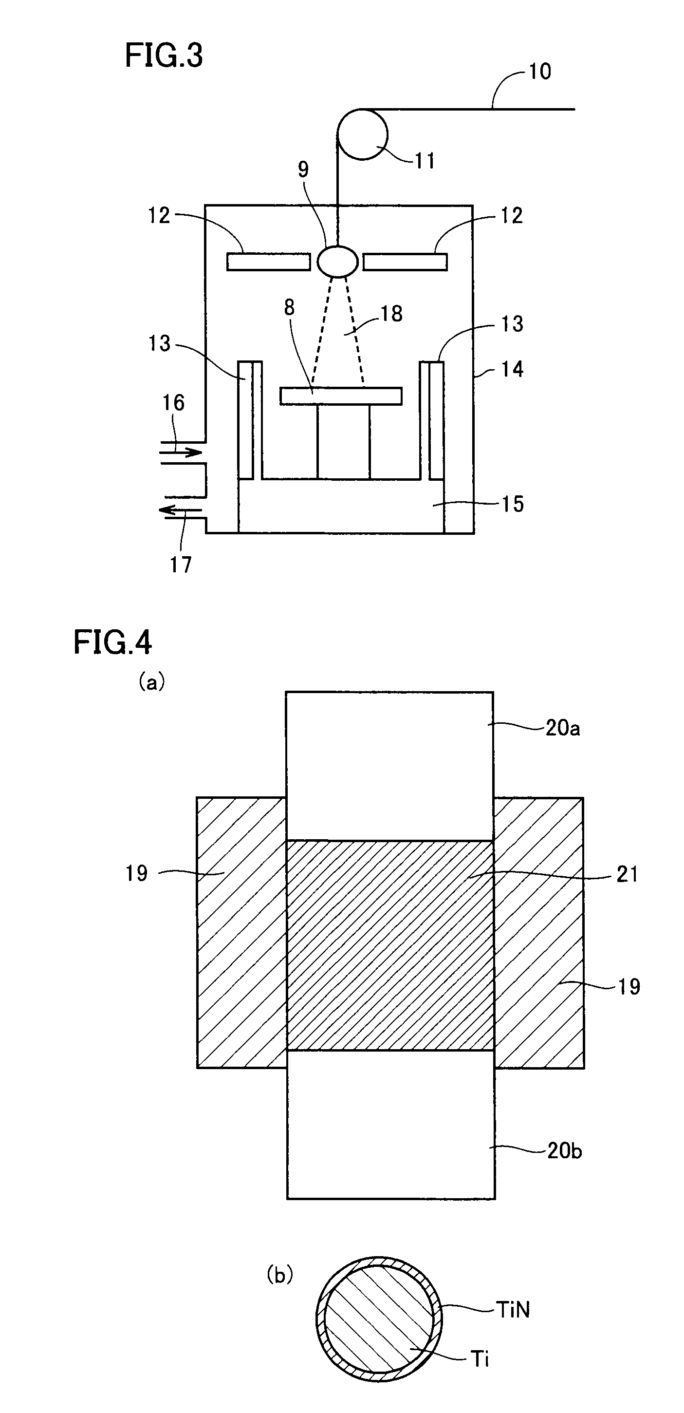
[0042]By the method shown in FIG. 3 in which a plasma atomizing method and a rotary disk process are combined, a titanium wire having a line width of 0.3 mm was molten by plasma torch 12 for granulation. At that time, rotary disk 8 was rotated at 100 krpm to manufacture fine titanium particles having a mean particle size of 20 μm. The fine particles were manufactured under vacuum.
[0043]While the obtained fine titanium particles were retained in chamber 14 set to be under a vacuum condition as shown in FIG. 3, nitrogen was introduced therein as a nitriding gas. Heater 13 was heated to 800° C. to thereby form a titanium nitride coating at a surface of the fine titanium particles (see FIG. 4(b)). An observation was conducted on the thickness of the coating on the obtained particles by means of an Auger electron spectroscopy measurement device having a sputtering function, showing that a nitride coating having a mean thickness of 20 nm was formed.
[0044]As shown in FIG. 4(a), the fine ti...
example 2
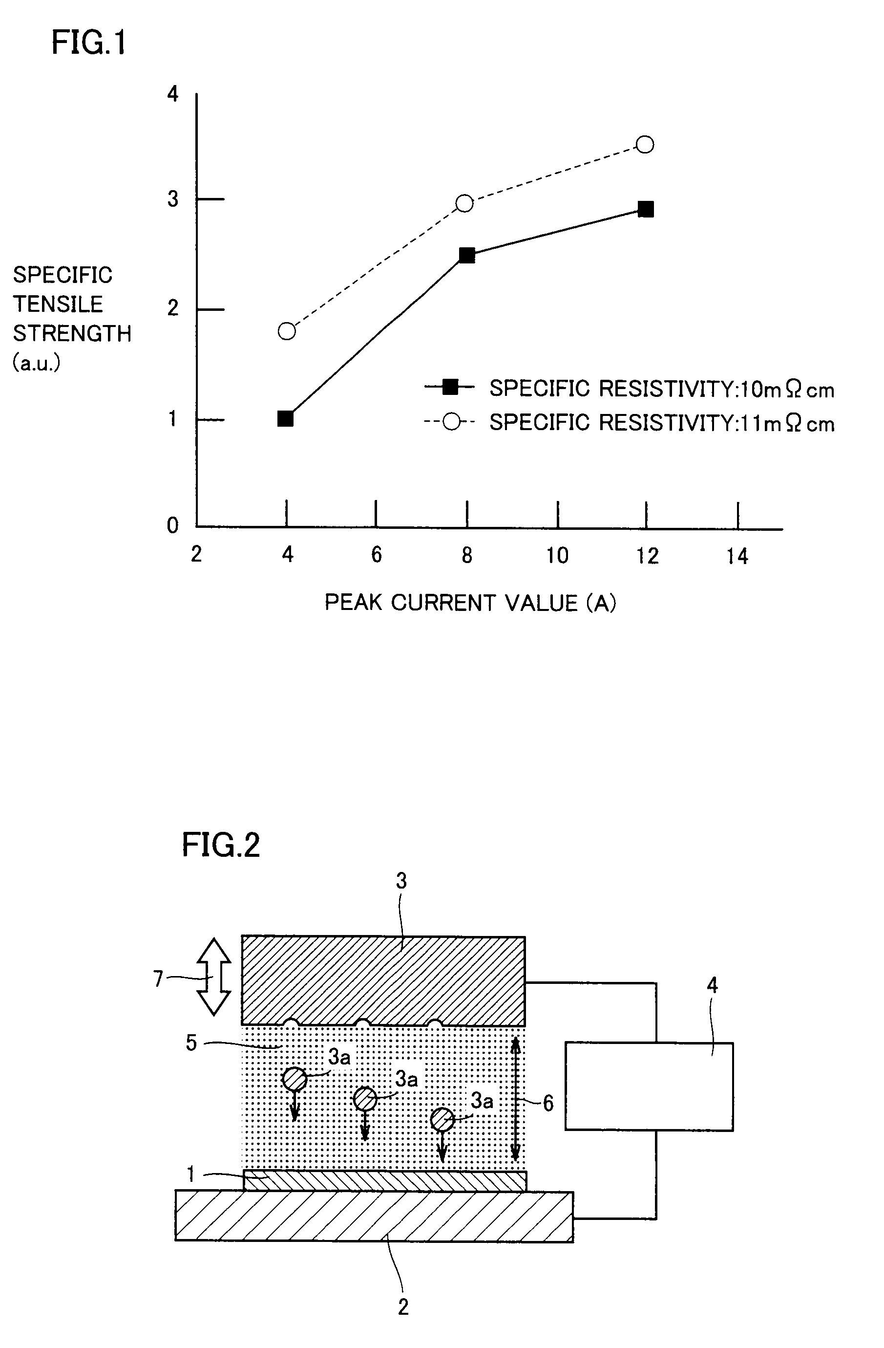
[0054]As shown in Example 1, the electrical discharge surface treatment was conducted with a peak current value ie=10 (A), an electrical discharge duration (electrical discharge pulse width) te=64 (μs), and pause time to=128 (μs), by allowing the electrode having an area of 10 mm×10 mm to scan on a substrate (100 mm×100 mm) made of a titanium 64 alloy, to form an electrical discharge surface treatment coating that was made of pure titanium and had a thickness of 100 μm, in a region of 50 mm×50 mm.
example 3
[0059]As shown in Example 1, the electrical discharge surface treatment was conducted with a peak current value ie=10 (A), an electrical discharge duration (electrical discharge pulse width) te=64 (μs), and pause time to=128 (μs), by allowing the electrode having an area of 15 mm×15 mm to scan on a turbine blade formed of a titanium 64 alloy, to form an electrical discharge surface treatment coating made of pure titanium and having a film thickness of 500 μm.
[0060]After the electrical discharge surface treatment coating was formed, its surface was ground with use of a grinder. The ultimate thickness of the titanium electrical discharge surface treatment coating was 300 μm.
PUM
| Property | Measurement | Unit |
|---|---|---|
| Thickness | aaaaa | aaaaa |
| Thickness | aaaaa | aaaaa |
| Length | aaaaa | aaaaa |
Abstract
Description
Claims
Application Information