

Semiconductor device, method for producing the same, sensor and electro-optical device
- Summary
- Abstract
- Description
- Claims
- Application Information
AI Technical Summary
Benefits of technology
Problems solved by technology
Method used
Image

Examples
first embodiment
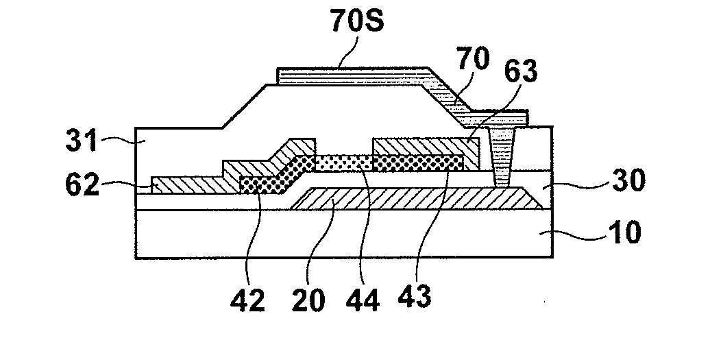
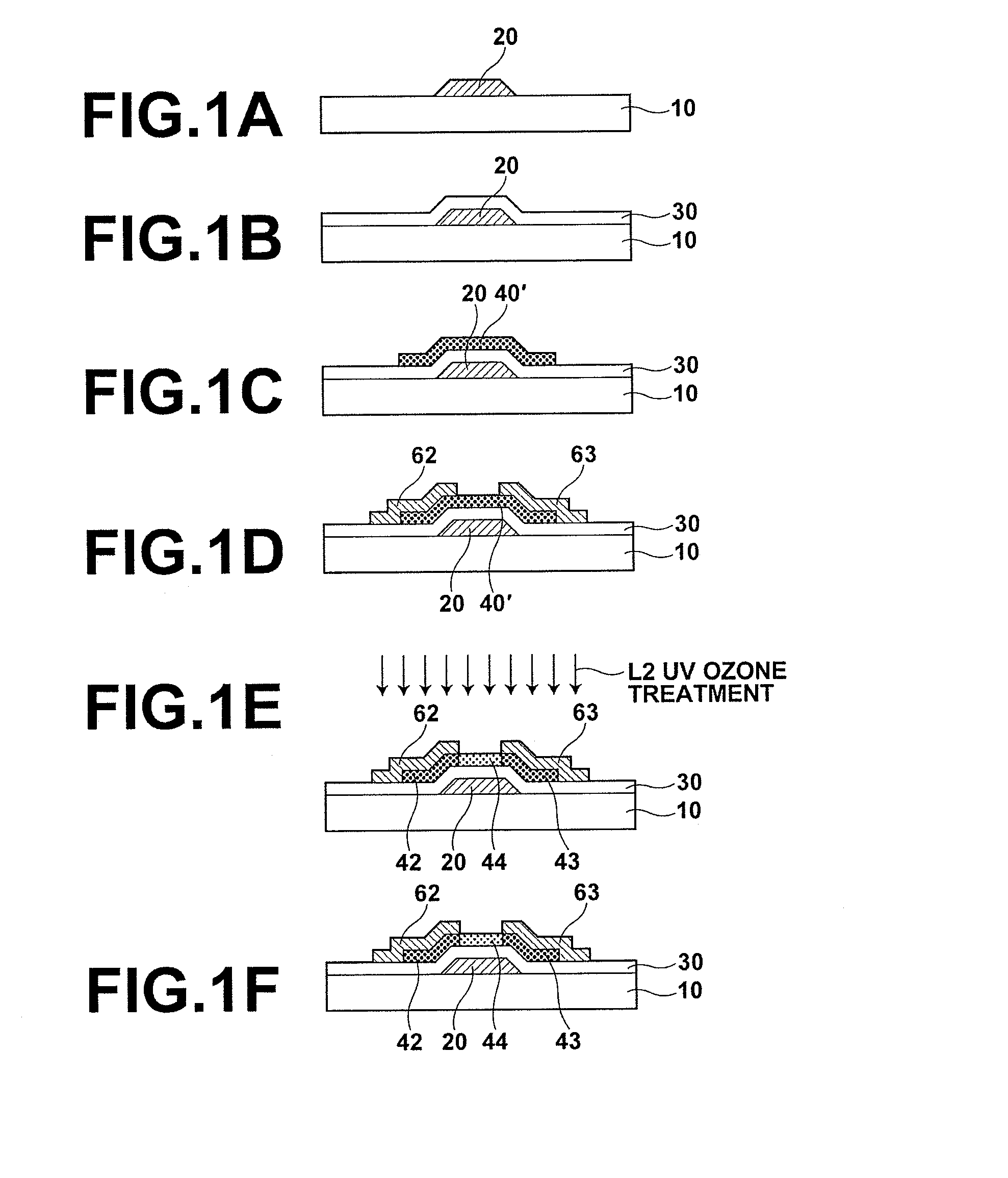
[0036]FIGS. 1A-1F are schematic sectional views illustrating the production flow of a method for producing a semiconductor device according to a first embodiment. FIG. 1F illustrates the semiconductor device produced by the production method according to this embodiment.
[0037]As shown in the drawings, in the method for producing a semiconductor device according to this embodiment, a patterned gate electrode 20 is formed on a substrate 10 (FIG. 1A), a gate insulation film 30 is formed (FIG. 1B), and an inorganic oxide film 40′ having a carrier density of 1019 / cm3 or more is formed through a dry process on the gate insulation film 30 so that the inorganic oxide film 40′ is positioned above the gate electrode 20 (FIG. 1C). Thereafter, a source electrode 62 and a drain electrode 63 are formed through a dry process to partially cover the inorganic oxide film 40′ (FIG. 1D), and oxidation treatment (in FIG. 1E, UV ozone treatment using ultraviolet light L2 is shown as an example) is applie...
second embodiment
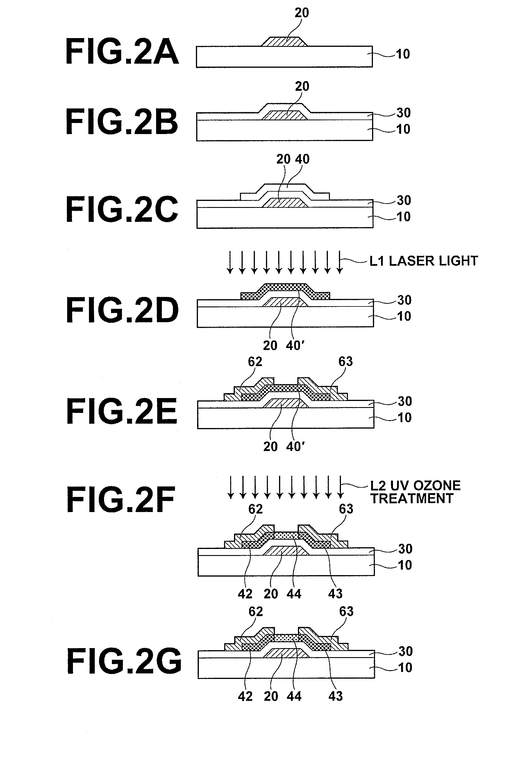
[0057]FIGS. 2A-2G are schematic sectional views illustrating the production flow of a method for producing a semiconductor device according to a second embodiment. FIG. 2G illustrates the semiconductor device produced by the production method according to this embodiment.
[0058]The method for producing a semiconductor device of this embodiment differs from the method of first embodiment in that, in the second embodiment, the inorganic oxide film 40′ is formed by a liquid phase method. The other features are the same as the first embodiment, and therefore, description of the same features as the first embodiment shown in FIG. 1 is omitted unless it is necessary.
[0059]As shown in the drawing, in the method for producing a semiconductor device according to this embodiment, the patterned gate electrode 20 is formed on the substrate 10 (FIG. 2A), the gate insulation film 30 is formed (FIG. 2B), an inorganic oxide film precursor 40 is formed through a liquid phase method on the gate insula...
third embodiment
[0085]FIGS. 3A-3G are schematic sectional views illustrating the production flow of a method for producing a semiconductor device according to a third embodiment. FIG. 3G illustrates the semiconductor device produced by the production method according to this embodiment.
[0086]The method for producing a semiconductor device of this embodiment differs from the method of the second embodiment in that the source electrode 62 and the drain electrode 63 are formed using a liquid phase method, in stead of the dry process. The other features are the same as the second embodiment, and therefore, description of the same features as the second embodiment shown in FIGS. 2A-2G is omitted unless it is necessary.
[0087]As shown in the drawing, in the method for producing a semiconductor device according to this embodiment, the patterned gate electrode 20 is formed on the substrate 10 (FIG. 3A), the gate insulation film 30 is formed (FIG. 3B), the inorganic oxide film precursor 40 is formed through ...
PUM
| Property | Measurement | Unit |
|---|---|---|
| Electrical resistance | aaaaa | aaaaa |
| Carrier concentration | aaaaa | aaaaa |
Abstract
Description
Claims
Application Information