Aa stacked graphene-diamond hybrid material by high temperature treatment of diamond and the fabrication method thereof

a technology of graphene and diamond, which is applied in the direction of polycrystalline material growth, after-treatment details, transportation and packaging, etc., can solve the problems of inability to assemble aa stacked graphene, etc., and achieves excellent physical properties, simple process, and maintain flatness in an atomic level

Inactive Publication Date: 2009-12-03
KOREA INST OF SCI & TECH
View PDF3 Cites 30 Cited by
  • Summary
  • Abstract
  • Description
  • Claims
  • Application Information

AI Technical Summary

Benefits of technology

[0023]According to the present invention, AA stacked graphene, having the interplanar spacing of 3.5˜4.4 Å which is greater than an existing AB stacked graphite (3.35 Å) by 5˜30% and having excellent physical properties, may be formed on a diamond matrix with a simple process.
[0024]According to the present invention, since there is no need to have a time to generate a nucleus on the diamond matrix (i.e., incubation time), a second unit process is enabled, and the graphene surface may maintain flatness in an atomic level.
[0025]The diamond serves as a nonconductor (insulator), and graphene has a characteristic of a semi-conductor or conductor. The AA stacked graphene-diamond hybrid material may be utilized in a next generation semi-conductor device (e.g., graphene-diamond single crystal substrate), an electrode material of a Li battery with enhanced power density (e.g., graphene-diamond powder), and various types of a new material development.

Problems solved by technology

However, the AB stacked graphene is more stable than the AA stacked graphene in terms of energy, whereby pure AA stacked graphene does not exist and even its composition is not possible.

Method used


Image

  • Aa stacked graphene-diamond hybrid material by high temperature treatment of diamond and the fabrication method thereof
  • Aa stacked graphene-diamond hybrid material by high temperature treatment of diamond and the fabrication method thereof
  • Aa stacked graphene-diamond hybrid material by high temperature treatment of diamond and the fabrication method thereof

Examples


example 1

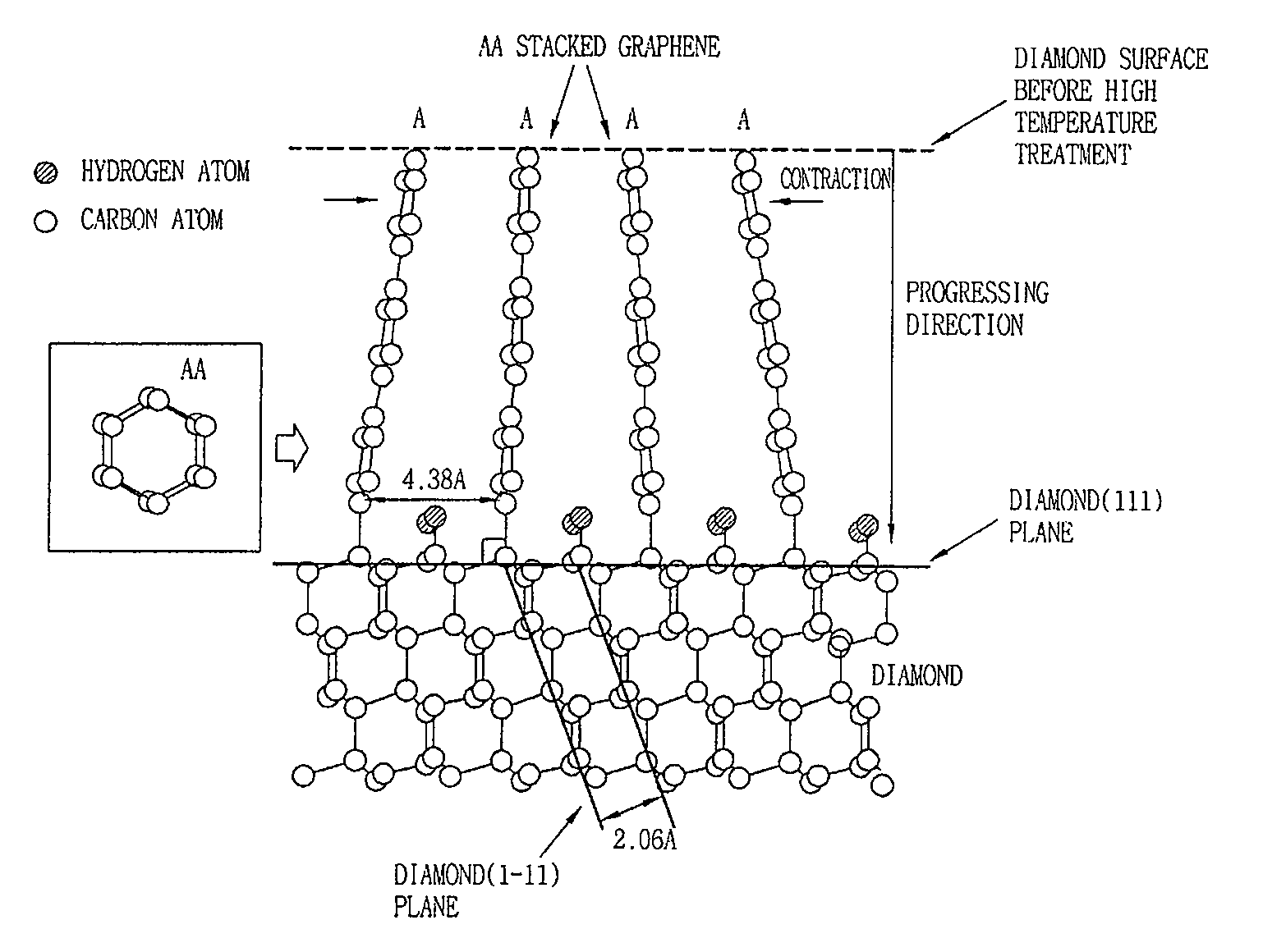
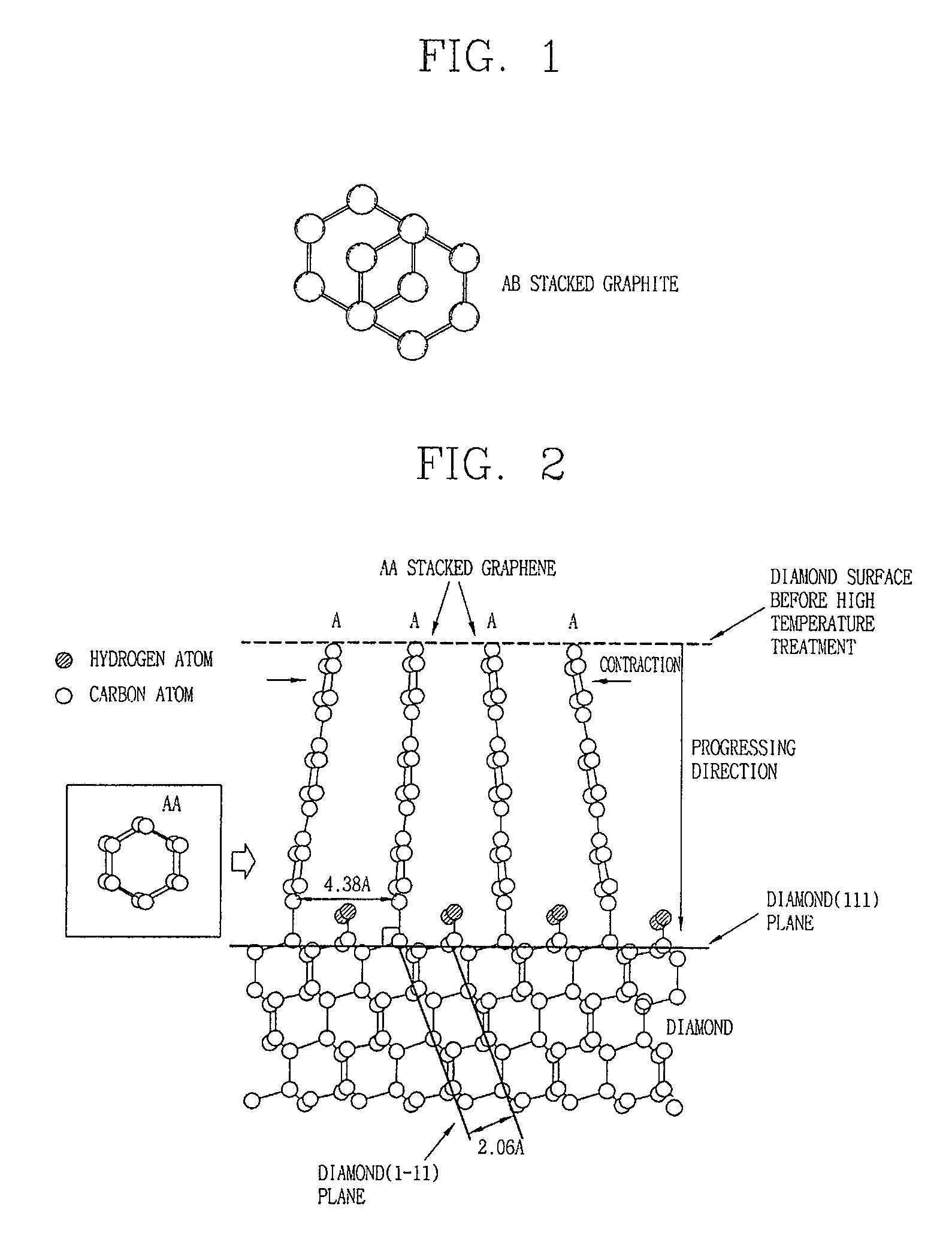
[0039]AA stacked graphene-diamond hybrid powder was prepared by using diamond powder (size: 1˜2 μm) as a matrix (refer to FIG. 6a).

[0040]A device used for the high temperature treatment was a multi-cathode direct current power plasma diamond synthesizer. After diamond powder was placed on to a molybdenum substrate, the diamond / substrate set was placed on an anode of the synthesizer for plasma treatment. The conditions of the plasma treatment are as follows: 200 sccm of hydrogen gas, a pressure of 100 Torr, and a molybdenum substrate at a temperature of approximately 1200° C. (Surface temperature of the diamond matrix is expected to be higher than that of the substrate by several tens ° C.). A processing time was 1 minute.

[0041]According to the result of analyzing this sample by X-Ray Diffraction (XRD), as shown in FIG. 7, a (001) peak (2θ=22.9°) of the AA stacked graphene, together with a diamond (111) peak (2θ=43.8°) and a (110) peak (2θ=75.4°) was observed. This indicated epitaxia...

example 2

[0042]A diamond / silicon plate in which diamond having a thickness of 5 μm was deposited on a silicon substrate having a diameter of 4″ and a thickness of 0.5 mm was used as a matrix (refer to FIG. 6b), and was undergone the plasma treatment for 10 seconds under the same condition as Example 1.

[0043]According to the result of analyzing the sample treated with the plasma by HRTEM, it could be observed that the thickness of the AA graphene layer was several nm, and the 2:1 conversion relationship between the diamond {111} lattice plane and graphene. Accordingly, the AA stacked graphene-diamond hybrid layer could be obtained on the silicon substrate.

example 3

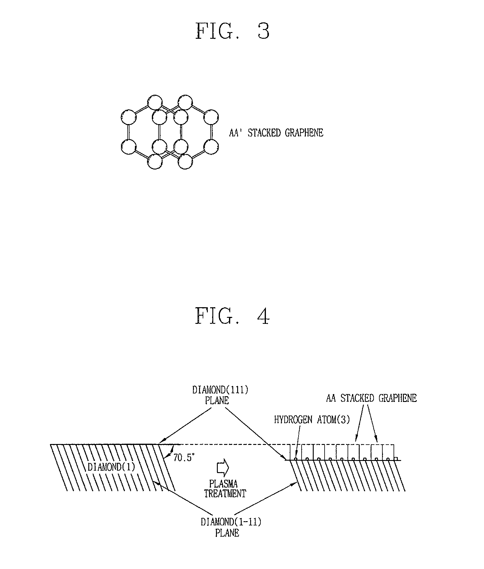
[0044]A polycrystalline CVD diamond film having a ground (abraded, polished) texture (10×10×0.5 mm3T) was used as a matrix, and was undergone the plasma treatment for 10 minutes under the same condition as Example 1 (here, the substrate temperature was 1250° C.).

[0045]According to the result of analyzing the treated sample by HRTEM, it was observed that the thickness of the AA graphene layer was several hundreds nm, and the 2:1 conversion relationship between the diamond {111} lattice plane and graphene. According to the result of analyzing this sample by rocking curve XRD, it was observed that graphene was oriented having an angle of 60° with respect to the diamond surface (i.e., (110) plane). This is identical to the schematic diagram as shown in FIG. 5. Accordingly, it could also be checked that the formation angle of AA stacked graphene was changed on the diamond as the surface constituting the diamond surface is changed.

[0046]Meanwhile, due to the structural characteristic of ...


PUM

PropertyMeasurementUnit
surface temperatureaaaaaaaaaa
temperatureaaaaaaaaaa

Abstract

There is provided a fabrication method for an AA stacked graphene-diamond hybrid material by converting, through a high temperature treatment on diamond, a diamond surface into graphene. According to the present invention, if various types of diamond are maintained at a certain temperature having a stable graphene phase (approximately greater than 1200° C.) in a hydrogen gas atmosphere, two diamond {111} lattice planes are converted into one graphene plate (2:1 conversion), whereby the diamond surface is converted into graphene in a certain thickness, thus to fabricate the AA stacked graphene-diamond hybrid material.

Description

RELATED APPLICATION[0001]The present disclosure relates to subject matter contained in priority Korean Application No. 10-2008-0050480, filed on 29 May, 2008, which is herein expressly incorporated by reference in its entirety.BACKGROUND OF THE INVENTION[0002]1. Field of the Invention[0003]The present invention relates to a high functional carbon material, and more particularly, to an AA stacked graphene-diamond hybrid material by high temperature treatment of diamond and a fabrication method thereof.[0004]2. Background of the Invention[0005]Graphene refers to one sheet of graphite, i.e., the (0001) surface of graphite. If graphene is stacked upon one another in a pattern of AB (or ABC), it becomes generally known graphite (space group #194, p6 / mmc; this is referred to as ‘AB stacked graphite’) (refer to FIG. 1). An interplanar spacing between graphene of the AB stacked graphite is 3.35 Å.[0006]If an element, such as Li, and the like, is intercalated into the AB stacked graphite, a ...

Claims


Application Information

Patent Timeline
Patent Type & Authority Applications(United States)
IPC IPC(8): B32B9/00B01J19/12B82B1/00B82B3/00
CPCB01J3/006B01J19/088B01J2219/0809B01J2219/0879B01J2219/0894Y10T428/30C01B31/06C01B31/065C30B29/04C30B33/02C01B31/04C01B32/26C01B32/28C01B32/182C01P2004/80
Inventor LEE, JAE-KAPLEE, SO-HYUNGLEE, SEUNG-CHEOLAHN, JAE-PYOUNGLEE, JEON-KOOKLEE, WOOK-SEONG
Owner KOREA INST OF SCI & TECH
Why Eureka
Try Eureka