Eureka AIR delivers breakthrough ideas for toughest innovation challenges, trusted by R&D personnel around the world.

Color controlled electroluminescent devices

a technology of electroluminescent devices and color control, which is applied in the direction of packaging, natural mineral layered products, synthetic resin layered products, etc., can solve the problems of less reliable and efficient, impede the efficient transport of charge carriers, and achieve the effect of improving color stability and light-emitting efficiency, and not hindering the charge transport properties of the matrix

Inactive Publication Date: 2009-12-17
TECHNION RES & DEV FOUND LTD
View PDF6 Cites 13 Cited by
  • Summary
  • Abstract
  • Description
  • Claims
  • Application Information

AI Technical Summary

Benefits of technology

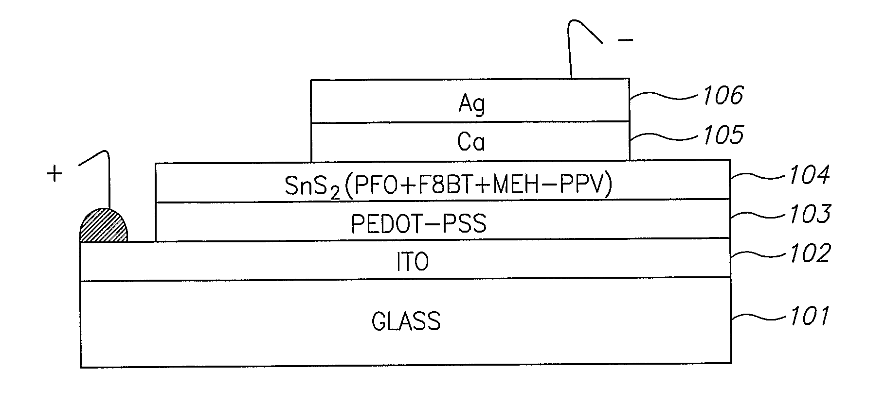
[0008]The present invention seeks to provide a new organic electroluminescence scheme utilizing a single nanocomposite material, comprising a number of different luminescent polymer components incorporated into a layered matrix, such that chain-chain interactions are hindered, and energy transfer among the components by Forster energy transfer and by exciton diffusion is inhibited. The matrix is preferably constructed of a semiconducting material, such that the charge transport properties of the matrix are not hindered. The prevention of energy transfer between the different incorporated components means that exciton recombination occurs radiatively at each of the locations where the excitons are formed, each location being associated with its own component, thereby enabling essentially simultaneous emission of the color associated with each local component, and without significantly influencing the emission of neighboring components. Once such a situation is achieved, it becomes possible to synthesize any color emission required, whether white or of a specific color, by a simple selection procedure of the component mixture concentrations. Such a scheme enables the preparation of organic electroluminescent (hereinafter EL) white-light-emitting materials with improved color stability and light-emitting efficiency. Additionally, such a scheme enables the “tuning” of the material to a specific desired emitted wavelength region by means of a readily predetermined mixture of the EL-active material components.
[0009]Preferably, the host matrix is a semiconductor or a blend of semiconductor and insulators. Use of an insulating matrix, as described in the Park et al prior art, may provide transparency for the emitted light, but it may impede the efficient transport of the charge carriers. The semi-conducting matrix of the present invention, on the other hand, though it may absorb some of the emitted light, is capable of transporting the carriers, thus enabling significantly more efficient and simpler operation of devices constructed using these materials. A balanced blend of two host matrices may preferably be used. According to preferred embodiments of the present invention, tin sulphide SnS2 may be used as a semiconductor matrix material, with or without the addition of MoO3 as an insulator matrix material. The use of solely insulator host matrices may be envisioned, but would likely entail the application of higher fields in order to render such devices operational, and hence may be less reliable and less efficient. This is apparent from the article by J. H. Park et al, entitled “Stabilized Blue Emission from Polymer-Dielectric Nanolayer Nanocomposites” published in Adv. Funct. Mater., Vol. 14, No. 4, pp. 377-382 (April 2004), and in the article by M. Eckel and G. Decher, entitled “Tuning the Performance of Layer-by-Layer Assembled Organic Light Emitting Diodes by Controlling the Position of Isolating Clay Barrier Sheets” published in Nonoletters, Vol 1(1), pp. 45-49 (2001), from where it can be seen that the reported the turn-on fields of such devices with insulating layered hosts, are considerably higher than those of similar devices made using semiconductor layered hosts, such as are reported in the article by some of the inventors of the present application, entitled “Stable Blue Emission from a Polyfluorine / layered Compound Guest / host Nanocomposite”, presented at the 6th. International Symposium on Functional pi-Electron Systems, Cornell University, Ithaca, June 2004, and published in Adv. Funct. Mater., Vol. 16, No. 7, pp. 980-986 (April 2006).
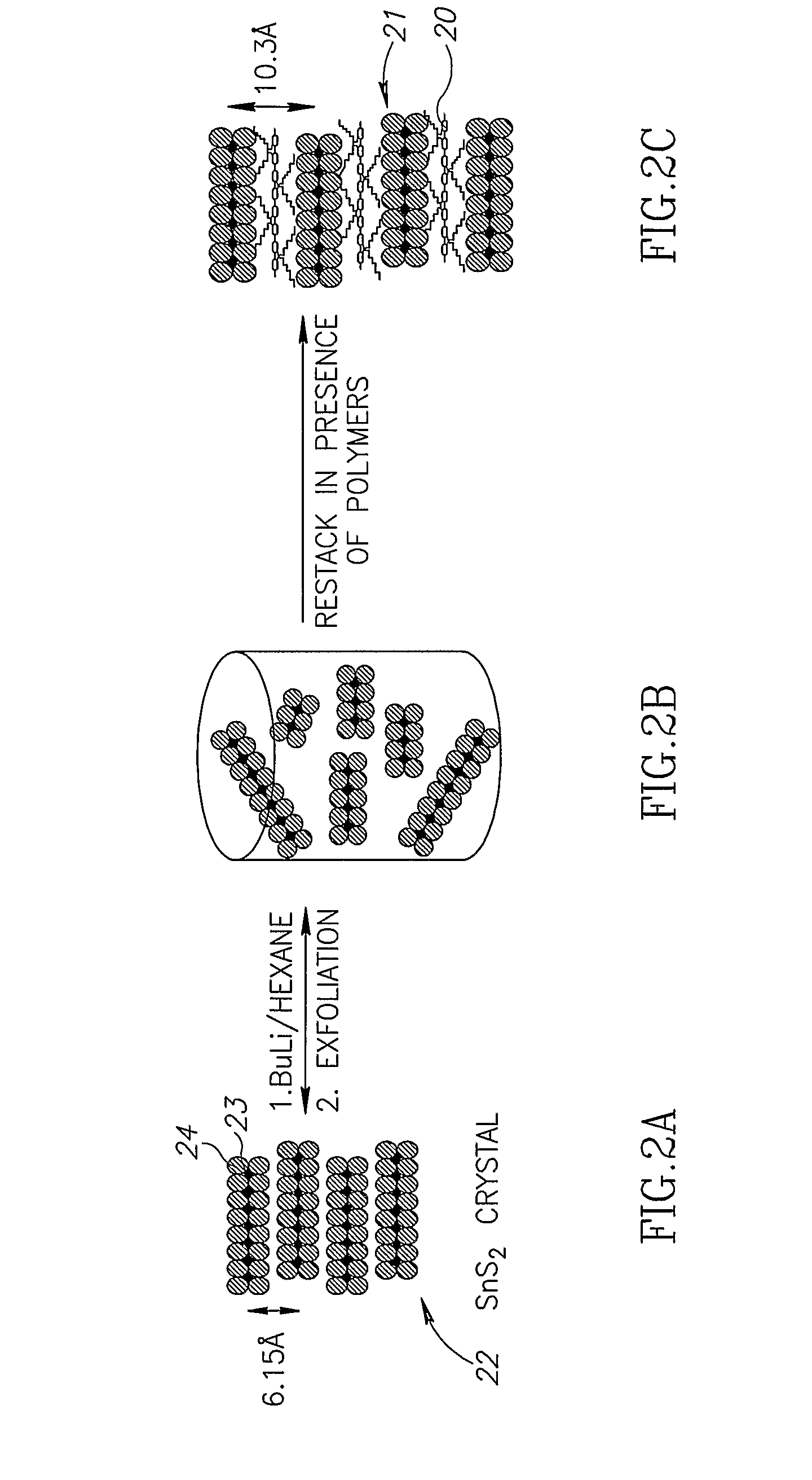
[0013]Confinement of the conjugated polymer chains within the spatially restrictive planar galleries of the layered matrix material is believed to provide molecular property benefits that can be exploited to promote controlled wavelength emission, whether white or of a preselected color. The layered matrix enforces an extended planar morphology conformation on the polymer monolayer, and at the same time, significantly reduces polymer aggregation and π-π interchain interactions including charge and energy transfer. Specifically, strong interactions between the conjugated molecular guest material and the semiconductor matrix sheets prevent the π-stacking of polymer chains. It is known that the π-π interactions are responsible for the efficient energy transfer in polymer films, owing to high inter-chain exciton hopping rates. Consequently, the reduced inter-chain interactions arising from the diminished π-stacking is expected to hinder the energy transfer between polymer chains accommodated within a single host grain or even within a single gallery. Therefore, even in the “composite of blends” type of nanocomposite, where energetic interaction may have been expected between different mixed polymer species incorporated within a single gallery, this mechanism appears to be effective in reducing such interaction, and in maintaining the essentially independent emission of each species. It is also possible that inhibited exciton diffusion is also achieved by reduction of the exciton life-time due to interactions with the matrix.

Problems solved by technology

Use of an insulating matrix, as described in the Park et al prior art, may provide transparency for the emitted light, but it may impede the efficient transport of the charge carriers.
The use of solely insulator host matrices may be envisioned, but would likely entail the application of higher fields in order to render such devices operational, and hence may be less reliable and less efficient.

Method used


Image

  • Color controlled electroluminescent devices
  • Color controlled electroluminescent devices
  • Color controlled electroluminescent devices

Examples


Embodiment Construction

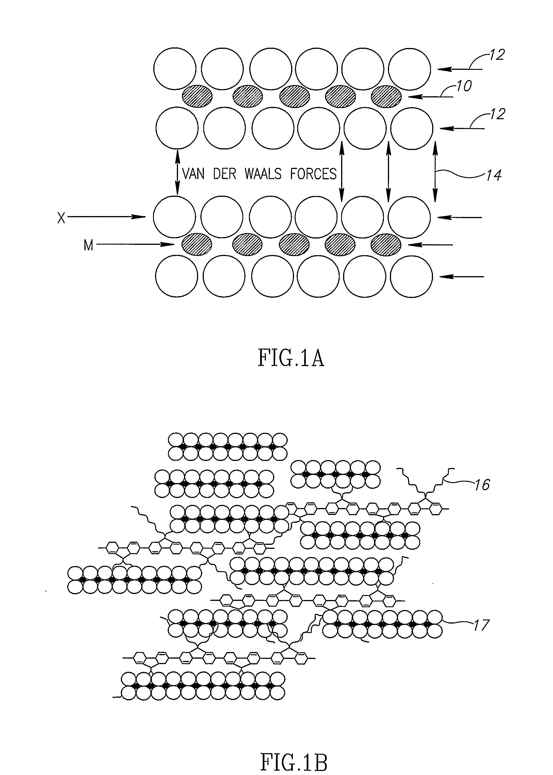
[0061]Reference is now made to FIG. 1A, which illustrates schematically an example of an inorganic layered host matrix, suitable for incorporating the active organic EL materials used in the present invention. The matrix comprises metal atoms and chalcogen atoms, and is shown in FIG. 1A as a dichalcogenide layer-type structure, though layered metal monochalcogenides may also be used. The layered metal dichalcogenides may have the chemical formula MX2 wherein M represents a metal and X represents a chalcogen, such as oxygen, sulfur, selenium or tellurium. The structure of the layered metal dichalcogenides preferably includes one sheet 10 of metal atoms sandwiched between two sheets 12 of chalcogen atoms. In the layered metal dichalcogenides, the metallic component M is preferably selected from the transition metals such as titanium, zirconium, hafnium, vanadium, tantalum, niobium, molybdenum and tungsten or some non-transition metals, preferably tin. More preferred chalcogens are sul...


PUM

PropertyMeasurementUnit
percentage weight ratioaaaaaaaaaa
excitation wavelengthaaaaaaaaaa

Abstract

An organic electroluminescent device of a composite material that includes at least two emissive polymers confined into a layered inorganic host matrix, which effectively isolates the polymer chains from their neighbors, and a method for manufacturing same. The isolation of the emitting chains inhibits energy transfer and exciton diffusion between polymer chains, such that the electrically generated excitons recombine radiatively before their energy could be funneled to the emissive moiety with the lowest band gap. The emission color of such a composite is a combination of the emission of the confined polymers, and can be either white light, or can be tuned by selection of the ratio of the mixtures to output light of any desired color. The different polymers can either be mixed and then intercalated into the host matrix, or they can each be intercalated separately into the host matrix and the resulting composites mixed.

Description

FIELD OF THE INVENTION[0001]The present invention relates to materials and methods for electroluminescent device construction and the control of the color output thereof, especially for use in white light emission devices, and for devices in which the emission color is selected by simple composition changes of the electroluminescent material.BACKGROUND OF THE INVENTION[0002]The commercial interest in cheap, large area, efficient white-emitting devices for display back-lighting and alternative solid-state lighting has focused attention towards solution-processed polymer light-emitting diodes (PLEDs). Two mechanisms have been proposed for the generation of white light in a polymer device. In the first approach, charges recombine radiatively in discrete polymer layers each emitting in a different color. Simultaneous emission from several layers at once provides the desired white emission. Such multilayered device methods have been described by Kido et al. [J. Kido, M. Kimura, K. Nagai,...

Claims


Application Information

Patent Timeline
Patent Type & Authority Applications(United States)
IPC IPC(8): H01L51/54B32B9/00B32B27/30B32B27/00H01J1/63B32B37/00B32B38/16
CPCC09K11/06H01L51/0036H01L51/0037H01L51/0038H01L51/0039Y10T156/10H01L51/5036H05B33/10H05B33/14H05B33/20Y02B20/181H01L51/0043Y10T428/3154Y10T428/31855Y02B20/00H10K85/114H10K85/115H10K85/1135H10K85/151H10K85/113H10K50/125
Inventor FREY, GITTIAHARON, EYALKALINA, MICHAEL
Owner TECHNION RES & DEV FOUND LTD
Why Eureka
Eureka Blog
Learn More