Semiconductor device and manufacturing method thereof
- Summary
- Abstract
- Description
- Claims
- Application Information
AI Technical Summary
Benefits of technology
Problems solved by technology
Method used
Image


Examples
embodiment examples
[0036]Specific embodiment examples of this invention will be described in detail with reference to the drawings.
first embodiment example
MIM Structure 1 Incorporated in ULSI Wiring
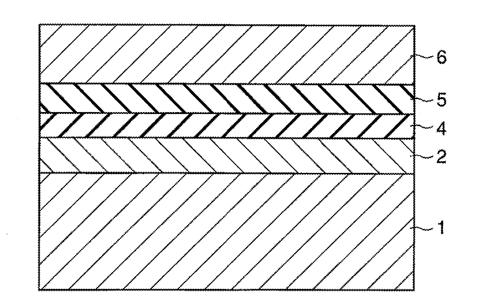
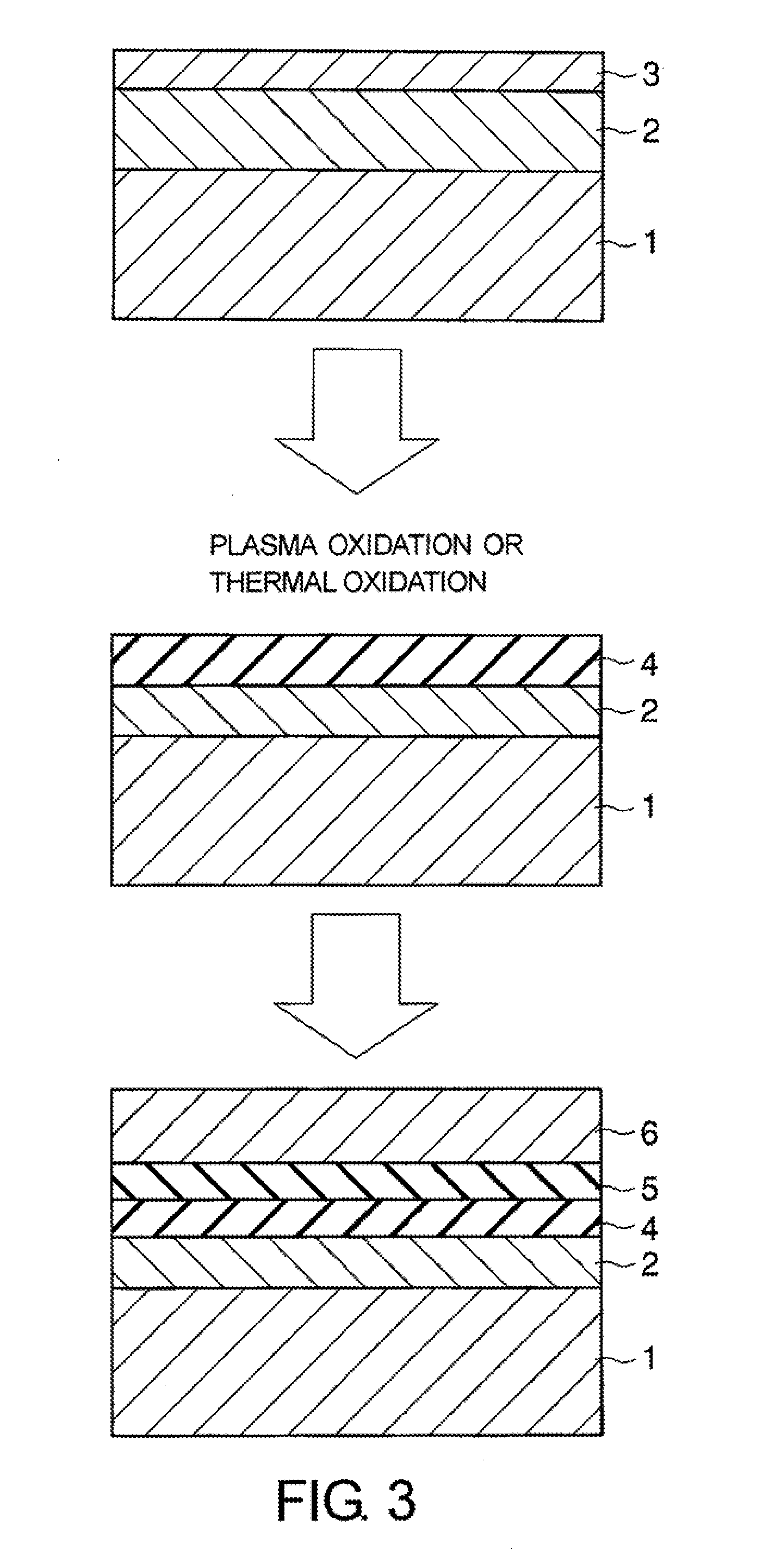
[0037]As shown in FIG. 6, a first embodiment example relates to an MIM structure incorporated in an actual ULSI wiring structure.
[0038]First, a 200-nm thick silicon oxide film 102 is formed on lower wiring 101 by plasma CVD. A 140-nm thick polycrystalline titanium nitride film 103 is formed as a lower electrode, a 5- to 10-nm thick tantalum film 104 is formed as a thin metal film, and a 5-nm thick tantalum nitride film 105 is formed. After that, the tantalum nitride film is plasma oxidized to produce a tantalum oxy-nitride film 106. The single layer of the tantalum film 104 may be oxidized by nitrogen monoxide (N2O) plasma to form a tantalum oxy-nitride film. A 100-nm thick titanium nitride film 107 is formed as an upper electrode film (FIG. 6(a)). The titanium nitride film 103, the tantalum film 104, the tantalum nitride film 105, and the titanium nitride film 107 can be formed by sputtering or CVD deposition method.
[0039]Subsequently as s...
second embodiment example
MIM Structure 2 Incorporated in ULSI Wiring
[0042]The MIM structure according to this invention may be manufactured by a method using a hard mask film. This method will be described with reference to FIG. 7.
[0043]First, in the same manner as shown in FIG. 6(a), a 200-nm thick silicon oxide film 202 is formed on lower wiring 201 by plasma CVD. A 140-nm thick titanium nitride film 203 is formed as a polycrystalline film, and a 10-nm thick tantalum film 204 and a 5-nm thick tantalum nitride film 205 are formed as thin metal films. The tantalum nitride film 205 is then plasma oxidized to form a tantalum oxy-nitride film 206. A 100-nm thick titanium nitride film 207 is formed as an upper electrode film. Further, a 100-nm thick silicon nitride film 208 is formed as a hard mask film by plasma CVD (FIG. 7(a)). The combination of materials for the hard mask film 208 and the upper electrode film 207 may be selected such that the upper electrode film 207 is resistant to etching when the hard ma...
PUM
 Abstract
Description
Claims
Application Information