
Sn-b plating solution and plating method using it

Inactive Publication Date: 2010-02-18
ILJIN COPPER FOIL
View PDF10 Cites 5 Cited by
  • Summary
  • Abstract
  • Description
  • Claims
  • Application Information

AI Technical Summary

Benefits of technology

[0028]According to the present invention, a Sn—B alloy plating layer that does not generate whisker can be provided.
[0029]Atoms of B are relatively small compared to atoms of Sn, and thus the atoms of B can penetrate into interstitial sites of Sn as will be described later. Accordingly, when a plating solution containing Sn and B forms a plating layer on a lead frame formed of Cu, Cu can be prevented from being diffused into the Sn, and thus generation of whisker on the plating layer is prevented. Consequently, electrical short circuits in a semiconductor lead frame having a plating region containing Sn and B including the Sn—B alloy plating layer is prevented, and durability of an electrical device using the semiconductor lead frame is improved.
[0030]A plating solution of Sn and B can generate a smooth plating surface. In the event of external shock, ductility of a smooth plating surface is better than a relatively rough plating surface. Also, a smooth plating surface can be transformed without any damage, and thus is suitable for providing a plating layer that can protect outer surface of an outer lead frame.
[0031]The plating solution of the present invention does not contain lead (Pb), and thus is harmless to the human body and is environmental friendly.
[0032]By using the plating solution of the present invention, the plating can be performed with relatively low current density at normal temperature, without separately heating the plating solution. Accordingly, productivity and profitability are improved.BEST MODE
[0033]As described above, in a conventional Sn type plating layer, whisker on the surface of the plating layer is a problem. However, reasons for the generation of whisker are not clearly understood.

Problems solved by technology

However, it is difficult to perform such a plating method, and the semiconductor chip often malfunctions due to plating solution penetrating between the surface of the semiconductor lead frame and epoxy molding.
Also, an additional process is required in order to remove un-uniformity of a plating layer.
However, when the base material is Cu or an alloy, such as alloy 42 that does not include a Cu component, the semiconductor lead frame badly corrodes.
Also, the price of Pd is unstable, and when the price of Pd increases, the manufacturing costs of the semiconductor package also increase.
However, a plating method used in the PPF method and the two-tone pre-plated frame method has several problems due to environmental contamination caused by lead.
However, in pure Sn plating, short circuits may be formed due to excessive generation of whisker.
The whiskers are vulnerable to heat and humidity.
When the whiskers are formed on the surface of the plating layer of a semiconductor lead frame, the semiconductor is electrically short circuited, and thus the circuit malfunctions.
However, the Sn—Bi alloy cannot sufficiently suppress the generation of whisker, and the deposition potential difference between Sn and Bi is significant, and thus eutectoid is difficult.
Also, when concentration of Bi in a solution is high, Bi is deposed on the surface of the cathode, and can fall off after soldering.
Also, when content of Bi in a plating layer is high, cracks may form in the plating layer when the plating layer is bent.

Method used


Image

  • Sn-b plating solution and plating method using it
  • Sn-b plating solution and plating method using it
  • Sn-b plating solution and plating method using it

Examples


embodiment 1

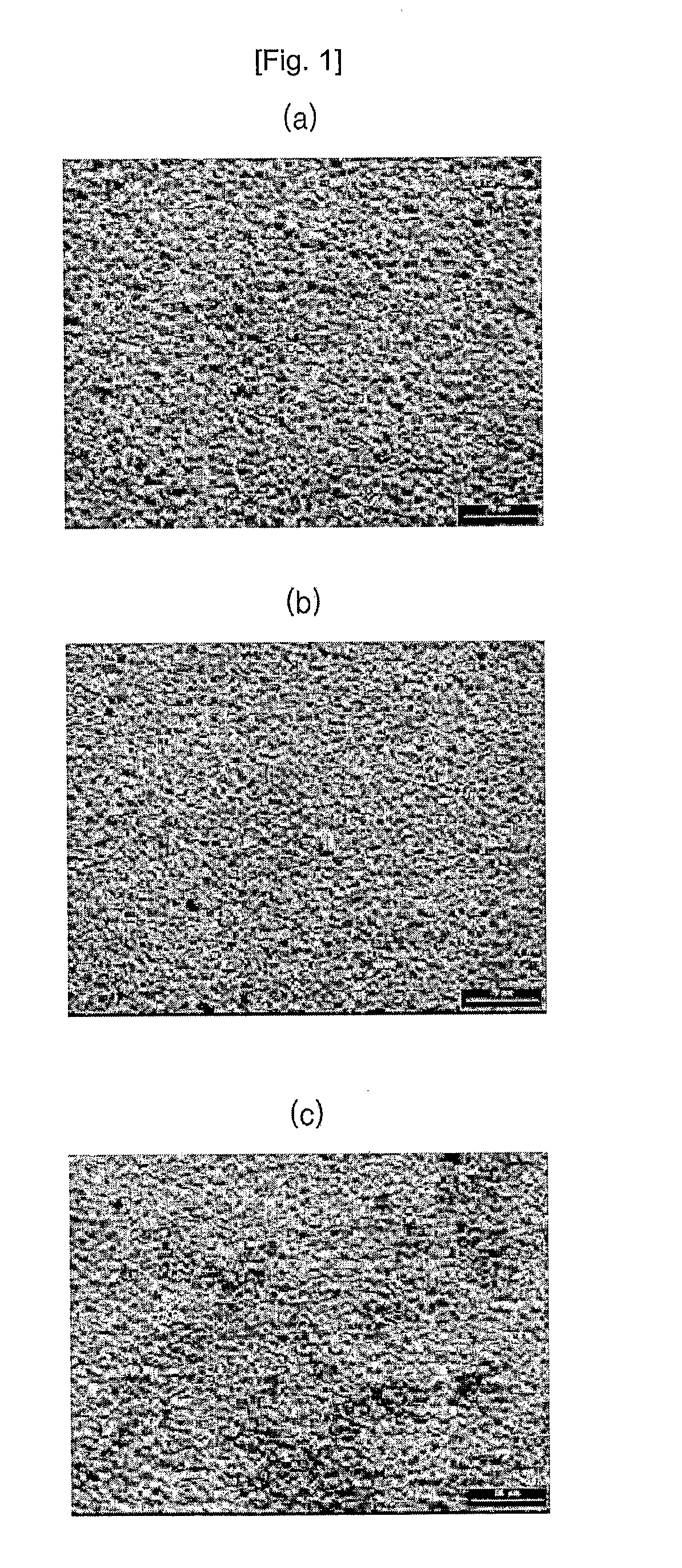
[0048]A plating solution containing 15 g / L of tin sulfate, 30 ml / L of H2SO4, 10 g / L of cresolsulfonic acid, 0.1 g / L of β-Naphtol, and 0.1 g / L of gelatin is produced.

[0049]In Experiment 1, 0.1 g / L of DMAB is further added to the plating solution, in Experiment 2, 0.5 g / L of DMAB is further added to the plating solution, and in Experiment 3, 3 g / L of DMAB is further added to the plating solution.

[0050]Plating is performed under the same plating conditions described above. In other words, a Cu plate is used as a cathode, soluble Sn is used as an anode, the current density is 1 A / dm2, and the plating temperature is normal temperature.

[0051]The plating layers of Experiments 1 through 3 are stored at room temperature for 12 months, and then it is determined whether whisker is generated on the surface of the plating layers.

[0052]FIGS. 1 (a) through (c) are scanning electron microscope (SEM) photographic images respectively illustrating surface states of the plating layers in Experiments 1 ...

embodiment 2

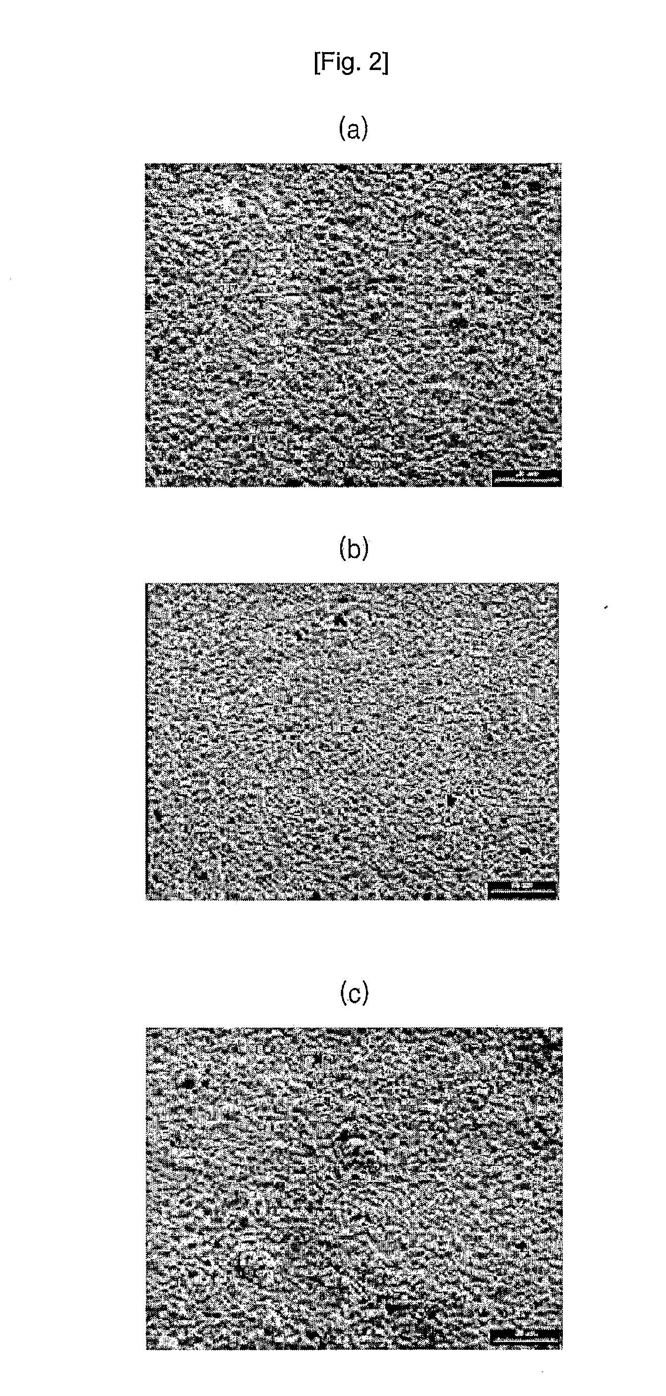
[0053]A plating solution containing 30 g / L of tin sulfate, 50 ml / L of H2SO4, 20 g / L of cresolsulfonic acid, 0.3 g / L of β-Naphtol, and 0.5 g / L of gelatin is produced.

[0054]In Experiment 4, 0.1 g / L of DMAB is further added to the plating solution, in Experiment 5, 0.5 g / L of DMAB is further added to the plating solution, and in Experiment 6, 3 g / L of DMAB is further added to the plating solution.

[0055]Plating is performed under the same plating conditions of Example 1. The is plating layers of Experiments 4 through 6 are stored at room temperature for 12 months, and then it is determined whether whisker is generated on the surface of the plating layers.

[0056]FIGS. 2 (a) through (c) are SEM photographic images respectively illustrating surface states of the plating layers in Experiments 4 through 6 after the room temperature storage test.

embodiment 3

[0057]A plating solution containing 50 g / L of tin sulfate, 70 ml / L of H2SO4, 40 g / L of cresolsulfonic acid, 0.5 g / L of β-Naphtol, and 1.0 g / L of gelatin is produced.

[0058]In Experiment 7, 0.1 g / L of DMAB is further added to the plating solution, in Experiment 8, 0.5 g / L of DMAB is further added to the plating solution, and in Experiment 9, 3 g / L of DMAB is further added to the plating solution.

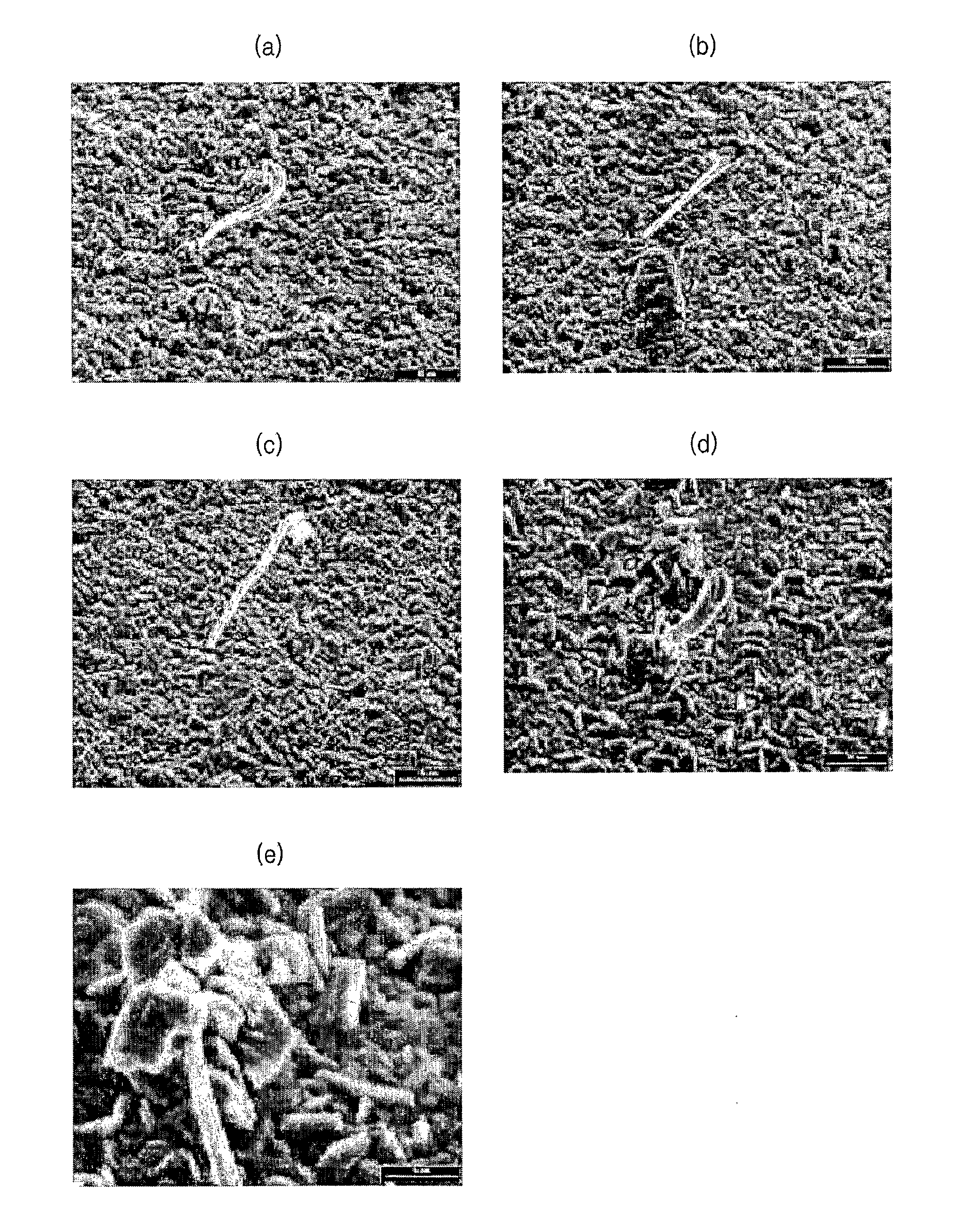
[0059]Plating is performed under the same plating conditions of Example 1. The plating layers of Experiments 7 through 9 are stored at room temperature for 12 months, and then it is determined whether whisker is generated on the surface of the plating layers.

[0060]FIGS. 3 (a) through (c) are SEM photographic images respectively illustrating surface states of the plating layers in Experiments 7 through 9 after the room temperature storage test.


PUM

PropertyMeasurementUnit
Densityaaaaaaaaaa
Densityaaaaaaaaaa
Densityaaaaaaaaaa

Abstract

The object of the present invention is to prevent generation of whisker in a Pb-free plating layer. Provided is a Pb-free Sn—B plating solution containing tin sulfate, which is a source of Sn ions, and dimethyl amine borane or trimethyl amine borane, which is a source of B ions.

Description

TECHNICAL FIELD[0001]The present invention relates to a Sn—B plating solution without lead (hereinafter, referred to as a Pb-free Sn—B plating solution), and a plating method using the same, and more particularly, to a Pb-free Sn—B plating solution that can prevent generation of whisker in a plating layer, and a plating method using the same.BACKGROUND ART[0002]The present invention does not contain lead, and at the same time, prevents generation of whisker in a plating layer. A semiconductor lead frame has various shapes depending on high densification or integration of the semiconductor chip, or a method of mounting the semiconductor chip on a substrate.[0003]Basically, the semiconductor lead frame is formed of a pad, in which a chip is mounted and maintains a static state of a chip thereon, i.e. a semiconductor memory device, an inner lead, which is connected to the chip by a wire bonding, and an outer lead, which connects the semiconductor lead frame to an external circuit. The ...

Claims


Application Information

Patent Timeline
IPC IPC(8): C25D3/30
CPCC25D3/60C25C3/30C25D3/30
Inventor LEE, DONG-NYUNGKIM, SANG-BEOMKANG, KYOO-SIK
Owner ILJIN COPPER FOIL
Learn More