Moisture detector, biological body moisture detector, natural product moisture detector, and product/material moisture detector

Active Publication Date: 2010-03-04
SUMITOMO ELECTRIC IND LTD
View PDF1 Cites 40 Cited by
  • Summary
  • Abstract
  • Description
  • Claims
  • Application Information

AI Technical Summary

Benefits of technology

[0027]The moisture detector may include an imaging device including a two-dimensional array of the light-receiving elements, and a moisture distribution image of the test object may be formed with the imaging device. Accordingly, a moisture distribution image of the test object that can be easily understood in terms of perception can be obtained.
[0028]The moisture detector may not include an artificial light source. A light-receiving portion o

Problems solved by technology

In the analysis performed by near-infrared spectroscopy, output signals include necessary information and a large amount of noise due to characteristics of a light-receiving element.
Accordingly, commercial devices including such photodiodes have a large size, and thus the photodiodes described in (1) are not suitable for handy-type or shoulder-type portable near-infrared spectrometers, digital cameras, or the like.
However, even when lead sulfide is used, the wavelength range in which light can be received is limited at room temperature.
InGaAs PIN photodiodes have a problem that the light-receiving sensitivity must be extended to the long-wavelength side of the near-infrared region.
However, this problem has not yet been satisfactorily solved in that noise and a dark current are suppressed while extending the light

Method used


Image

  • Moisture detector, biological body moisture detector, natural product moisture detector, and product/material moisture detector
  • Moisture detector, biological body moisture detector, natural product moisture detector, and product/material moisture detector
  • Moisture detector, biological body moisture detector, natural product moisture detector, and product/material moisture detector

Examples


first embodiment

Structure of Semiconductor Light-Receiving Element Array

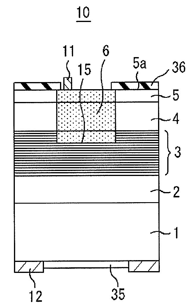
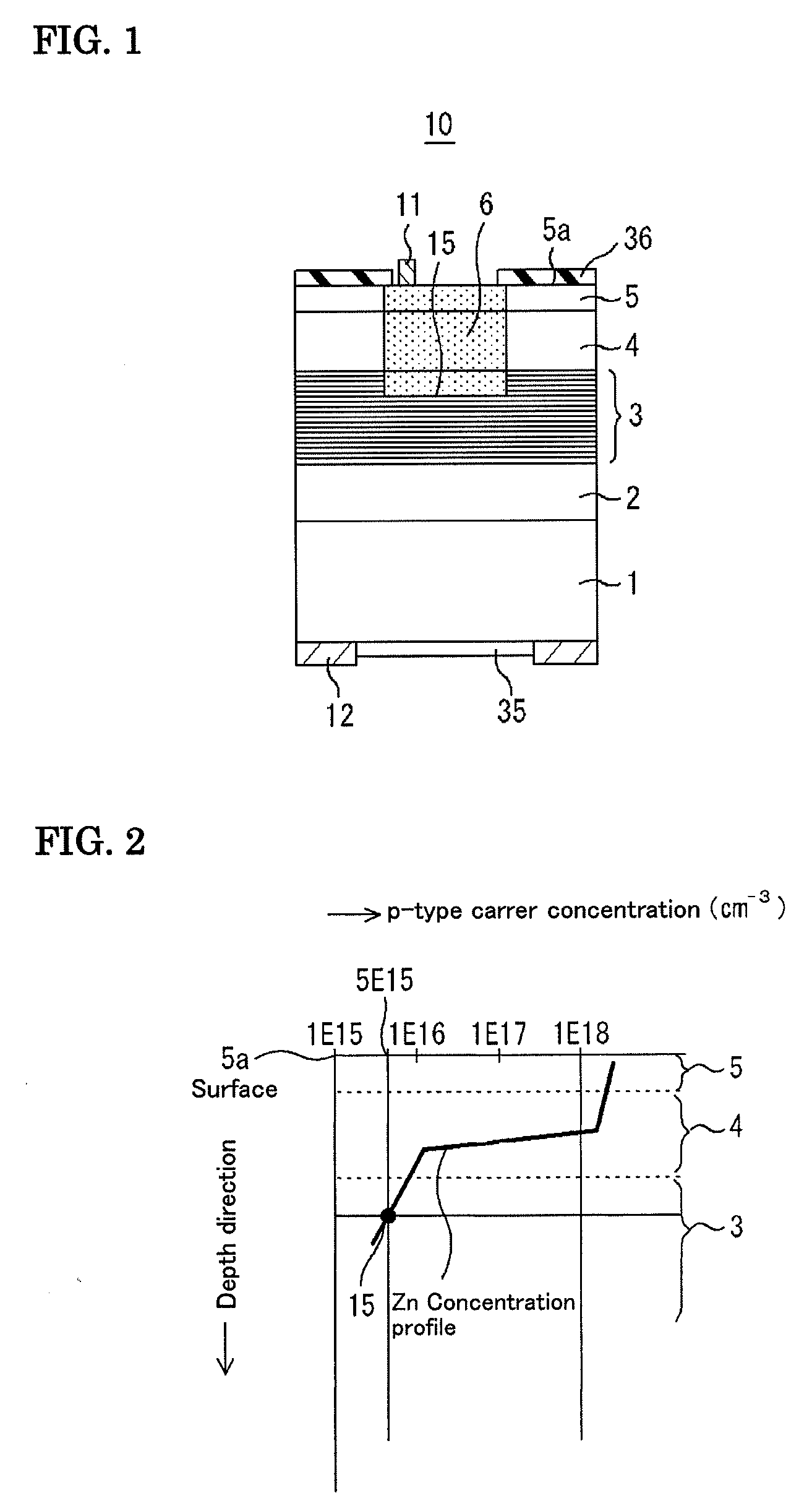
[0069]FIG. 1 is a cross-sectional view showing a light-receiving element 10 according to an embodiment of the present invention. Referring to FIG. 1, the light-receiving element 10 includes a Group III-V semiconductor laminated structure (epitaxial wafer) provided on a InP substrate 1. Specifically, the light-receiving element 10 has the following laminated structure:

(InP substrate 1, InP buffer layer 2, absorption layer 3 having a multiquantum well structure composed of InGaAs or GaInNAs and GaAsSb, InGaAs layer 4 for adjusting a concentration distribution of a diffused impurity, and InP window layer 5)

[0070]A p-type region 6 extending from the InP window layer 5 to the absorption layer 3 having the multiquantum well structure is formed by selectively diffusing Zn which is a p-type impurity from an opening of a selective diffusion mask pattern 36 composed of a SiN film. By performing diffusion using the selective diffusion mas...

second embodiment

Image Display (Imaging) of Moisture Distribution

1. The Structure of an Imaging Device (Moisture Distribution Imaging Device) in a Moisture Detector

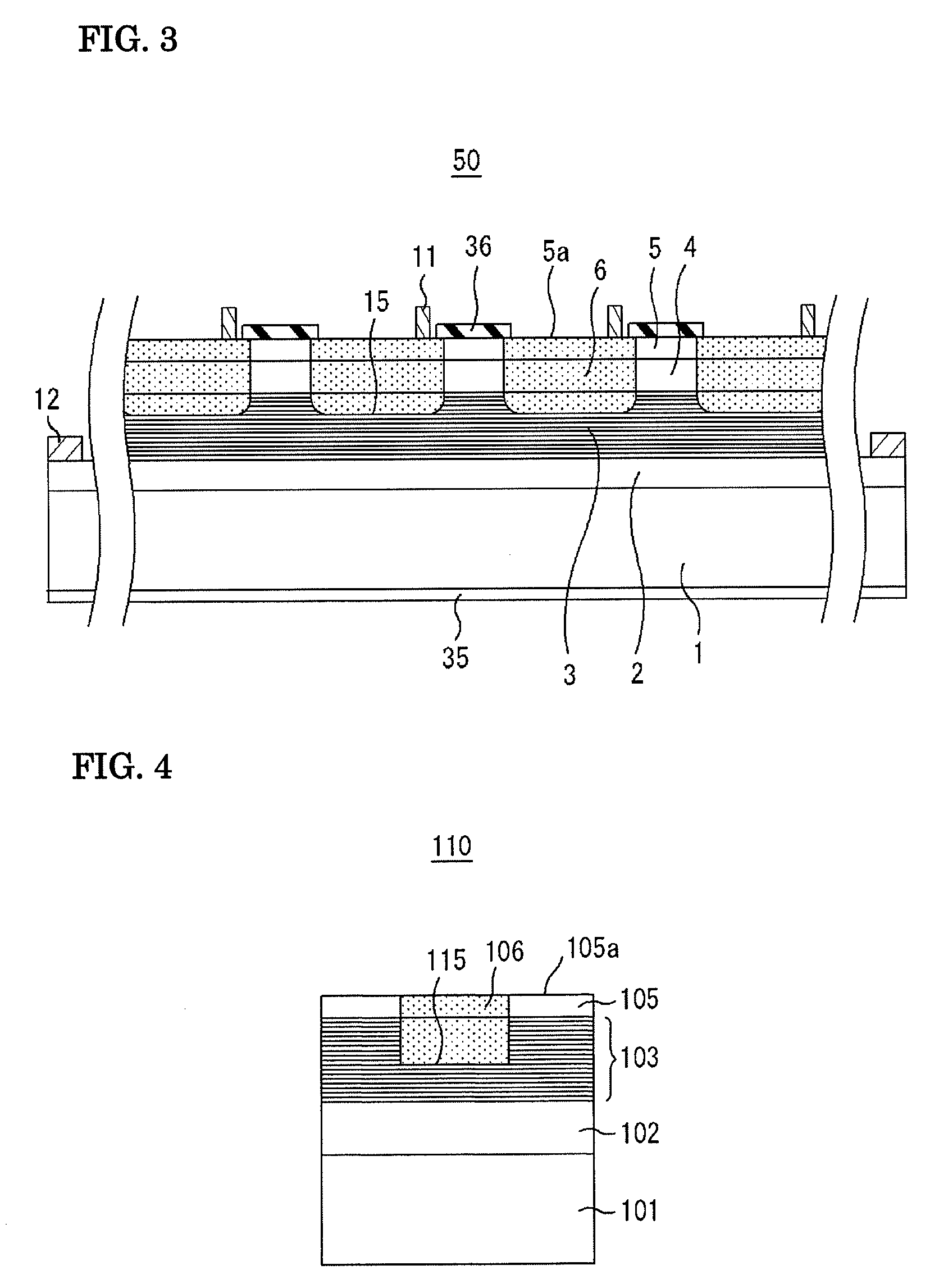
[0091]FIG. 8 is a view showing the outline of an imaging device (light-receiving element array) 70 included in a moisture detector according to a second embodiment of the present invention. Optical components such as a lens are omitted. FIG. 9 is a view illustrating the light-receiving element array 50 of the imaging device. FIG. 10 is a view showing a light-receiving element 10 in the light-receiving element array 50 shown in FIG. 9. In FIG. 8, in an imaging device 70, light-receiving elements 10 provided on a common InP substrate 51 are epi-side-down mounted so that an epitaxial layer side of the light-receiving elements 10 face a multiplexer 71 having a function of a mounting substrate. A p-side electrode 11 that is electrically connected to a p-type region 6 of the epitaxial layer of each of the light-receiving elements 10 and an n-si...

third embodiment

(1) Third Embodiment

Moisture Distribution Imaging Device for Melon Skin

[0099]For net melons having a striped pattern (net) on the skin, such as muskmelons, Yubari melons, and Andes melons, the appearance of the melons is evaluated before shipment. Hitherto, an image of a melon has been captured with a color camera, and the appearance has been evaluated by discriminating a net portion of the skin from a base portion thereof on the basis of color information of the color image. This evaluation method is disadvantageous in that the result is readily affected by a difference in color due to individual difference, or unevenness of illumination, and thus discrimination accuracy is low. Consequently, a difference in the moisture content between the base portion and a net portion of the skin of a melon has been paid attention, and a discrimination method using near-infrared light has been proposed. This method utilizes a fact that the moisture content of a base portion of the skin of a melo...


PUM


Abstract

A moisture detector includes a light-receiving element including an absorption layer having a pn-junction, or an array of the light-receiving elements, wherein the absorption layer has a multiquantum well structure composed of a Group III-V semiconductor, the pn-junction is formed by selectively diffusing an impurity element into the absorption layer, and the concentration of the impurity in the absorption layer is 5×10¹⁶/cm3 or less. The moisture detector receives light having at least one wavelength included in an absorption band of water lying in a wavelength range of 3 μm or less, thereby detecting moisture.

Description

BACKGROUND OF THE INVENTION[0001]1. Field of the Invention[0002]The present invention relates to a moisture detector, a biological body moisture detector, a natural product moisture detector, and a product / material moisture detector. More specifically, the present invention relates to a moisture detector, a biological body moisture detector, a natural product moisture detector, and a product / material moisture detector that include a light-receiving element having a high sensitivity to a long-wavelength region of the near-infrared region without cooling.[0003]2. Description of the Related Art[0004]Moisture, biological components, medicines, environmental materials, and the like have an absorption band in the near-infrared region, and thus near-infrared spectroscopy has attracted attention as a noninvasive analytical method, and studies and practical applications thereof have been intensively performed. In addition, cosmic light reaching the ground during the day and night has a plura...

Claims


Application Information

Patent Timeline
IPC IPC(8): H01L29/06B82Y10/00G01N21/01B82Y15/00B82Y20/00G01J1/02G01N21/3554H01L27/146H01L31/00H01L31/10
CPCB82Y20/00H01L31/03042Y02E10/544H01L31/035236H01L31/03046
Inventor IGUCHI, YASUHIRONAGAI, YOUICHI
Owner SUMITOMO ELECTRIC IND LTD
Why Eureka
Try Eureka