Manufacturing method of semiconductor device and manufacturing method of mask

Active Publication Date: 2010-04-01
RENESAS ELECTRONICS CORP +1
View PDF6 Cites 10 Cited by
  • Summary
  • Abstract
  • Description
  • Claims
  • Application Information

AI Technical Summary

Benefits of technology

[0012]As a result, when the EUV light is incident obliquely on the linear absorbers orthogonal to each other in a specified direction, the direction in which the shadow is cast and the direction in which the shadow is hardly cast are present. Since the region where the shadow is cast is the region where the absorber is not present and the multilayer film is exposed, the region is originally the region where the amount of reflection light of the EUV light is large, but the amount of reflection light of the EUV light from this region is reduced because the shadow is cast. This means that the resolution in the transfer of the pattern formed on the EUVL mask onto a semiconductor substrate is decreased. Furthermore, if the direction in which the shadow is cast and the direction in which the shadow is hardly cast

Problems solved by technology

In other words, in the lithography technique using the EUV light, the EUV light is absorbed by the material

Method used


Image

  • Manufacturing method of semiconductor device and manufacturing method of mask
  • Manufacturing method of semiconductor device and manufacturing method of mask
  • Manufacturing method of semiconductor device and manufacturing method of mask

Examples


first embodiment

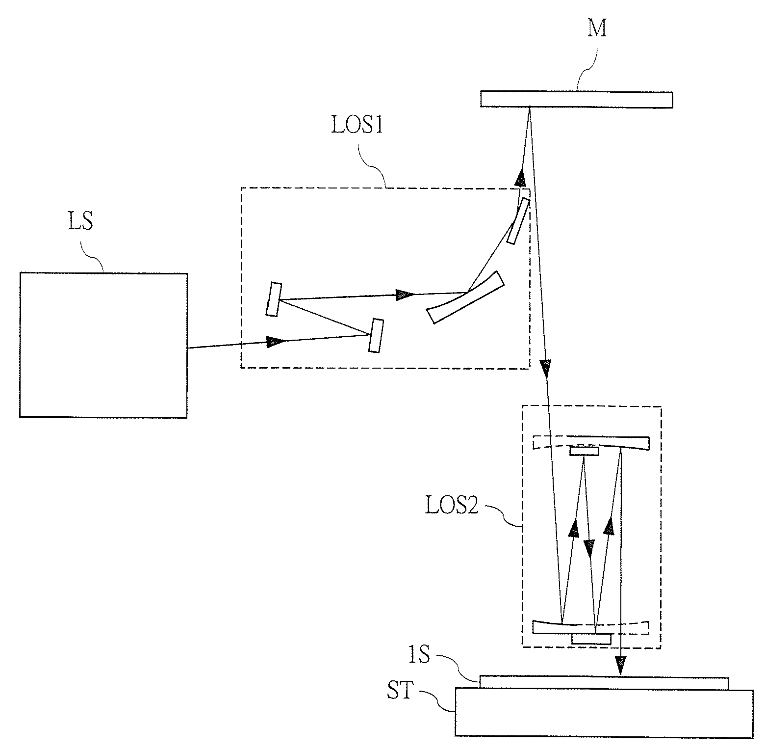
[0072]For example, the ArF lithography technique using argon fluoride (ArF) excimer laser light with the wavelength of 193 nm has been developed, and the lithography technique using the EUV light (EUVL (Extreme Ultra Violet Lithography)) with the much shorter wavelength of 13.5 nm (12 to 15 nm) has been under development so as to meet the requirement for the further scaling down of a pattern. In other words, since the more miniaturized pattern can be transferred onto a semiconductor wafer as the wavelength of the exposure light is shortened, the wavelength of the exposure light has been shortened for the transfer of the further miniaturized pattern.

[0073]At this time, in the normal photolithography technique using the argon fluoride (ArF) excimer laser light with the wavelength of 193 nm, the exposure light is transmitted through the mask having the circuit pattern formed thereon, thereby transferring the pattern formed on the mask onto a semiconductor substrate. That is, the mask i...

second embodiment

[0131]In the second embodiment, an example where high-density hole patterns are formed by using the mask manufactured in the first embodiment will be described. Similar to the first embodiment described above, the technique described in the second embodiment is based on the lithography technique in which EUV light is used and an exposure optical system in which the EUV light is obliquely incident on the mask is used.

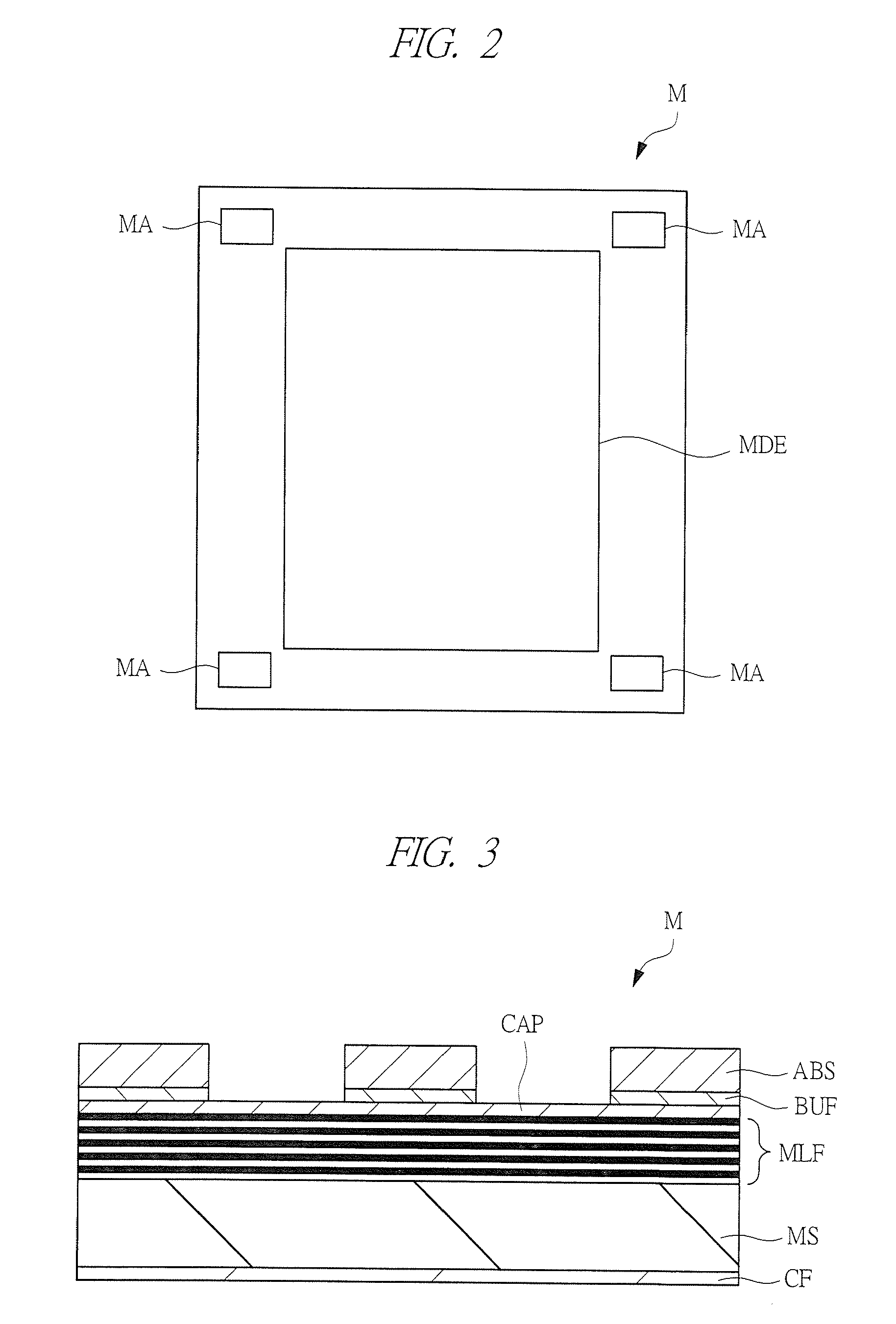
[0132]FIG. 27 is a diagram showing a part of a mask (corresponding to four holes) used for forming high-density hole patterns and an incident direction of an exposure light (incident light) on a mask surface. FIG. 27A shows a mask structure of a comparative example 1, in which four hole patterns are formed in the absorber ABS and the multilayer film MLF is exposed as a reflection region in the four hole patterns. The incident direction of the exposure light (incident light IL0) on the mask surface is as shown in FIG. 27A. FIG. 27B is a mask structure shown in the first e...

third embodiment

[0139]In the third embodiment, the manufacturing process of a semiconductor device including the process of forming the high-density hole patterns by using the mask manufactured in the first embodiment described above will be described with reference to the drawings. Similar to the first embodiment described above, the technique of forming the high-density hole patterns is based on the lithography technique in which EUV light is used and an exposure optical system in which the EUV light is obliquely incident on the mask is used.

[0140]FIG. 30 is a diagram showing a schematic layout structure of a whole semiconductor chip CHP in the third embodiment. In FIG. 30, an input-output circuit 1 is a circuit for providing an interface between an internal circuit region 2 including an internal circuit (core circuit) formed in an internal region of the semiconductor chip CHP and an external circuit formed outside the semiconductor chip CHP. A read only memory (ROM) 3, a clock pulse generator (C...


PUM


Abstract

Provided is a technique capable of improving the dimensional accuracy of a transfer pattern in a lithography technique in which EUV light is used and the EUV light is incident obliquely on a mask and an image of the EUV light reflected from the mask is formed on a semiconductor substrate (resist film), thereby transferring the pattern formed on the mask onto the semiconductor substrate. The present invention is based on a lithography technique in which EUV light is used and an exposure optical system in which the EUV light is obliquely incident on a mask is used. In this lithography technique, an absorber and a difference in level are formed on the mask, and a projective component projected on a mask surface out of a direction cosine component of the incident light is set to be almost orthogonal to an extending direction of the difference in level.

Description

CROSS-REFERENCE TO RELATED APPLICATION[0001]The present application claims priority from Japanese Patent Application No. JP 2008-254046 filed on Sep. 30, 2008, the content of which is hereby incorporated by reference into this application.TECHNICAL FIELD OF THE INVENTION[0002]The present invention relates to a technique for manufacturing a semiconductor device and a technique for manufacturing a mask. More particularly, it relates to a technique effectively applied to a photolithography technique using extreme ultra violet (hereinafter, referred to as EUV light) in a manufacturing process of a semiconductor device.BACKGROUND OF THE INVENTION[0003]Japanese Patent Application Laid-Open Publication No. 2004-96063 (Patent Document 1) describes a technique for providing a phase shift mask of EUV light that can be actually realized by obtaining an appropriate combination of a refractive index and an absorption coefficient even when reflecting the EUV light. More specifically, a phase shif...

Claims


Application Information

Patent Timeline
IPC IPC(8): G03F1/00G03F7/20G03F1/22G03F1/24H01L21/027
CPCB82Y10/00Y10T403/13G03F1/24B82Y40/00
Inventor TERASAWA, TSUNEOYAMANE, TAKESHI
Owner RENESAS ELECTRONICS CORP
Why Eureka
Try Eureka