

Thin film transistor and method for manufacturing the same
a thin film transistor and manufacturing method technology, applied in transistors, semiconductor devices, electrical equipment, etc., can solve the problems of not always improving element characteristics of a tft, unable to control nuclei generation positions and nuclei generation density directly, and no advantage over a polycrystalline silicon film formed, etc., to achieve the effect of reducing the off-state current and increasing the on-state current of the thin film transistor
- Summary
- Abstract
- Description
- Claims
- Application Information
AI Technical Summary
Benefits of technology
Problems solved by technology
Method used
Image

Examples
embodiment 1
[0058]In this embodiment, an example of a mode of a thin film transistor will be described with reference to the drawings.
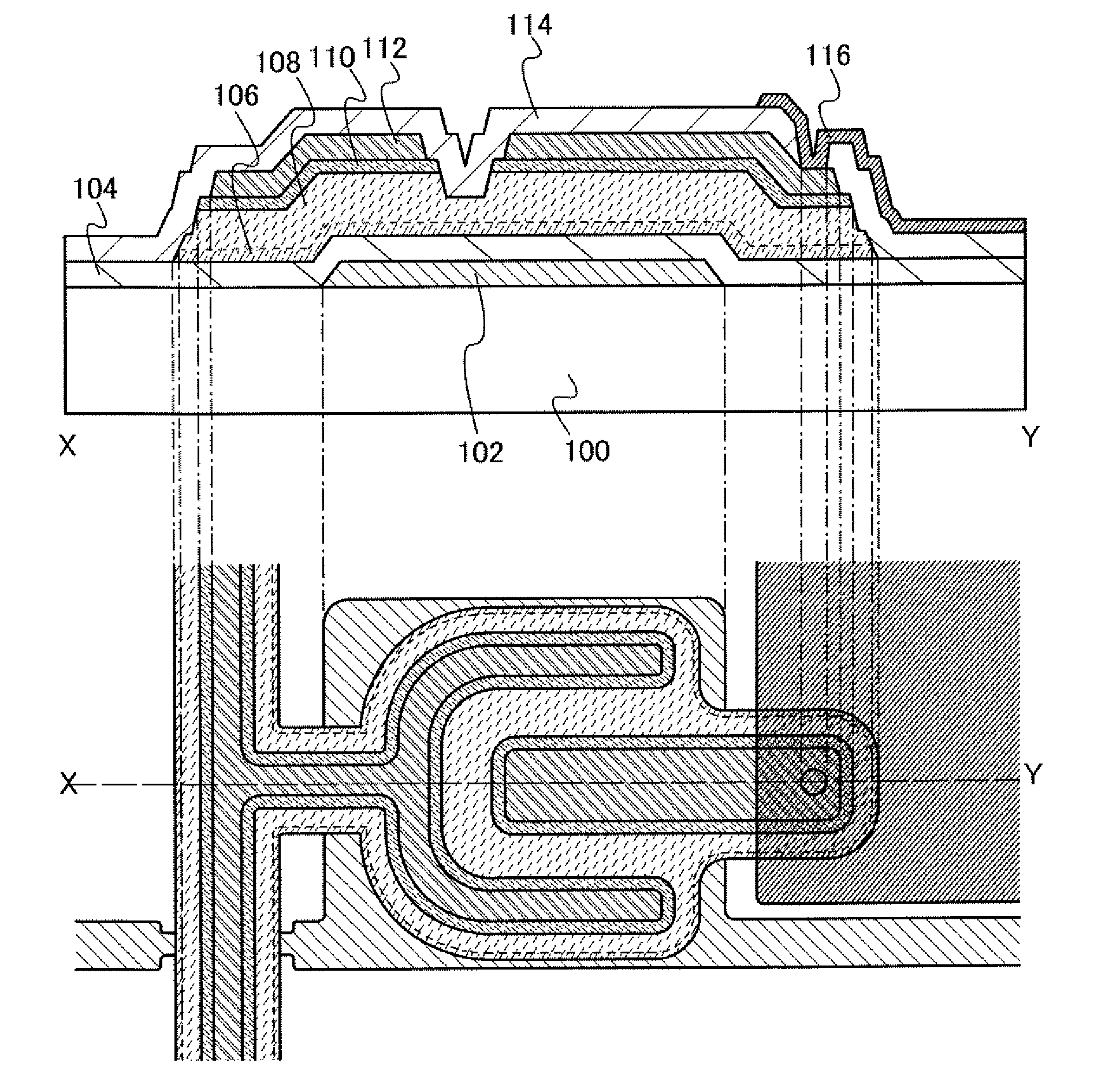
[0059]FIG. 1 is a top view and a cross-sectional view of a thin film transistor according to this embodiment. The thin film transistor illustrated in FIG. 1 includes a gate electrode layer 102 over a substrate 100; a gate insulating layer 104 covering the gate electrode layer 102; a semiconductor layer 106 provided over and in contact with the gate insulating layer 104; a buffer layer 108 over the semiconductor layer 106; and source and drain regions 110 provided over and in contact with the buffer layer 108. Further, the thin film transistor includes wiring layers 112 provided over and in contact with the source and drain regions 110. The wiring layers 112 form a source electrode and a drain electrode. The thin film transistor includes, over the wiring layers 112, an insulating layer 114 serving as a protective film. Further, each layer is patterned into a desir...
embodiment 2
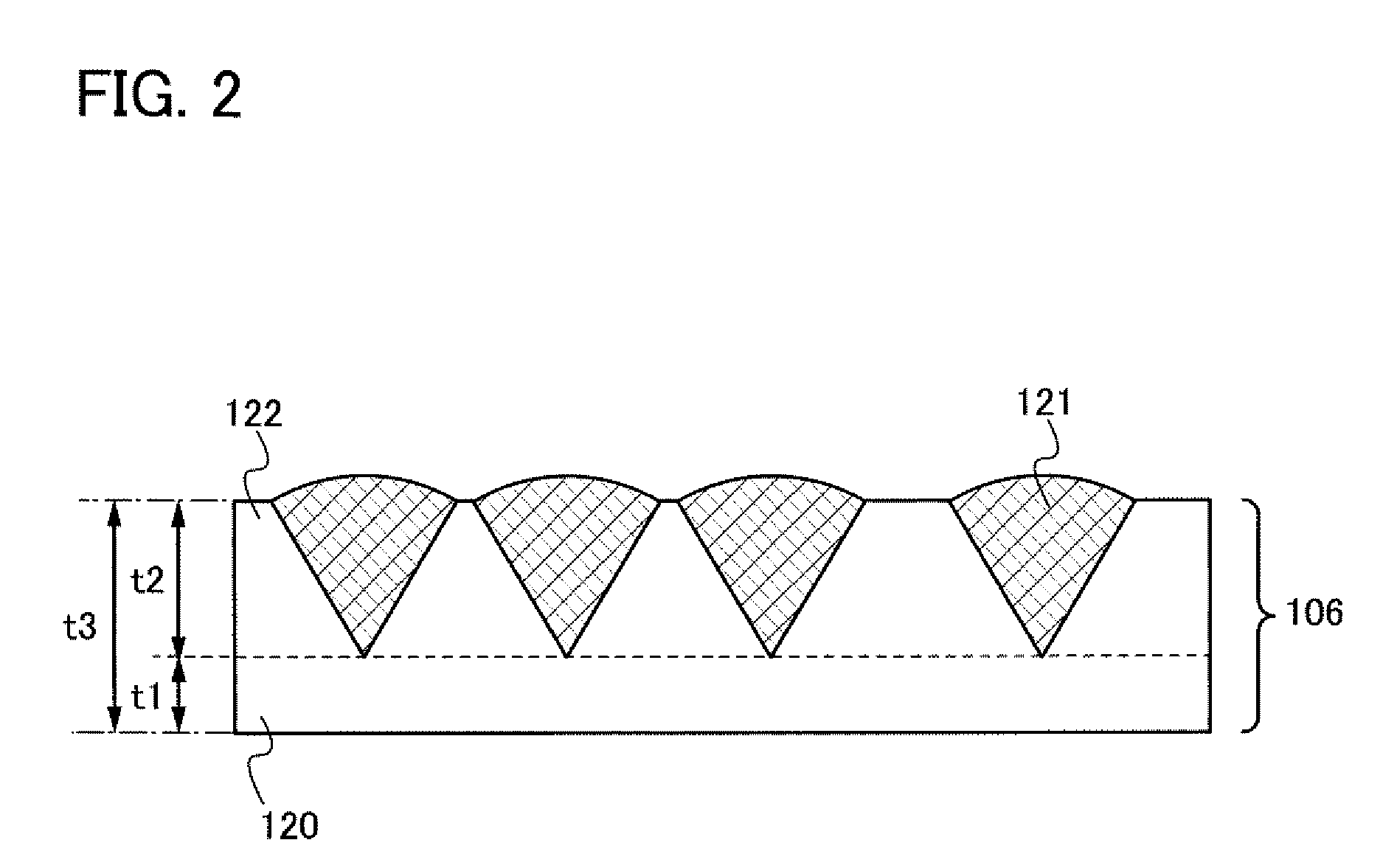
[0144]In this embodiment, a method for manufacturing the thin film transistor illustrated in FIG. 1, which is different from that of Embodiment 1, will be described. In this embodiment, a semiconductor layer including inverted conical or inverted pyramidal grains is formed in a manner similar to that of Embodiment 1. However, a method in which nitrogen is included in the semiconductor layer is different from that described in Embodiment 1.
[0145]In this embodiment, the gate insulating layer which is in contact with the semiconductor layer is formed using silicon nitride, whereby the concentration of nitrogen in the semiconductor layer is controlled, and the semiconductor layer including inverted conical or inverted pyramidal crystal particles is formed. A series of steps from a step of forming the gate insulating layer 104 to a step of forming the semiconductor layer 109 including an impurity element which serves as a donor will be described hereinafter with reference to FIG. 9.
[0146...
embodiment 3
[0155]In this embodiment, a method for manufacturing the thin film transistor illustrated in FIG. 1, which is different from those of Embodiments 1 and 2, will be described. In this embodiment, a semiconductor layer including inverted conical or inverted pyramidal grains is formed in a manner similar to those of Embodiments 1 and 2. However, a method in which nitrogen is included in the semiconductor layer is different from those described in Embodiments 1 and 2.
[0156]In this embodiment, the inside of the treatment chamber 141 is cleaned before a semiconductor layer is formed, and after that, the inner wall of the chamber is covered with a silicon nitride layer, whereby nitrogen is included in the semiconductor layer, the concentration of oxygen is suppressed low, and the concentration of nitrogen is made higher than the concentration of oxygen. A series of steps from a step of forming the gate insulating layer 104 to a step of forming the semiconductor layer 109 including an impuri...
PUM
 Abstract
Description
Claims
Application Information