

Sputtering Target and Oxide Semiconductor Film
a technology of semiconductor film and sputtering target, which is applied in the field of sputtering target and oxide semiconductor film, can solve the problems of defective film formation, increased production cost, and lowered sputtering targ
- Summary
- Abstract
- Description
- Claims
- Application Information
AI Technical Summary
Benefits of technology
Problems solved by technology
Method used
Image

Examples
first embodiment
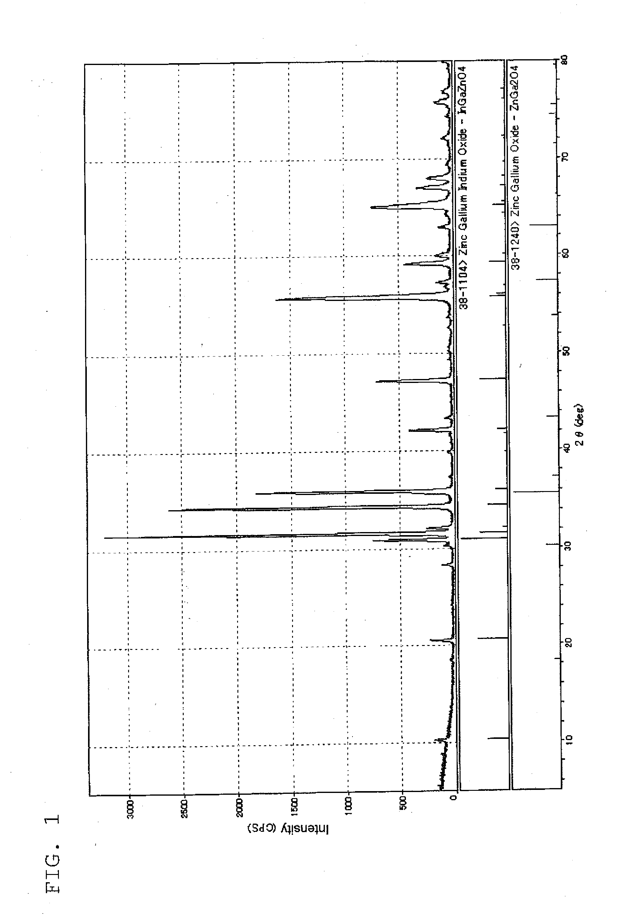
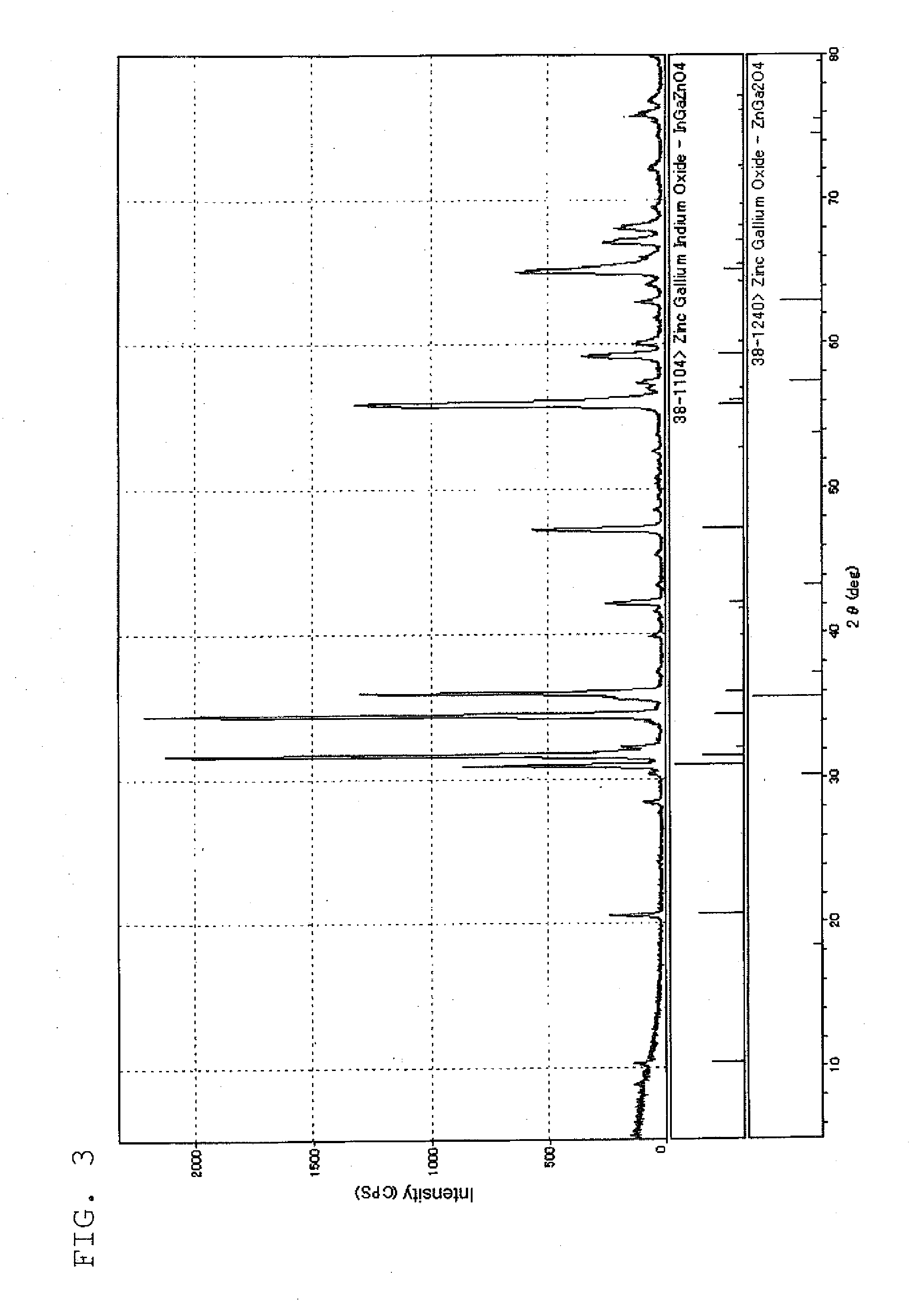
[0080]The sputtering target of the invention (hereinafter often referred to as “the target of the invention”) contains oxides of indium (In), gallium (Ga) and zinc (Zn), and comprises a compound shown by ZnGa2O4 and a compound shown by InGaZnO4.
[0081]By allowing a compound shown by ZnGa2O4 and a compound shown by InGaZnO4 to be generated in a sputtering target, abnormal growth of a compound shown by InGaO3(ZnO)m (wherein m is an integer of 2 to 20) can be suppressed, and abnormal discharge of the sputtering during sputtering can be suppressed. In addition, since the crystal particle size can be reduced, oxygen deficiency is generated in the crystal interface, whereby bulk resistance can be reduced.
[0082]In addition, the sputtering target of the invention contains a plurality of crystal systems such as a compound shown by InGaO3(ZnO)m (wherein m is an integer of 2 to 20) and a compound shown by ZnGa2O4, oxygen deficiency occurs due to the incommensuration of crystals in the crystal g...
second embodiment
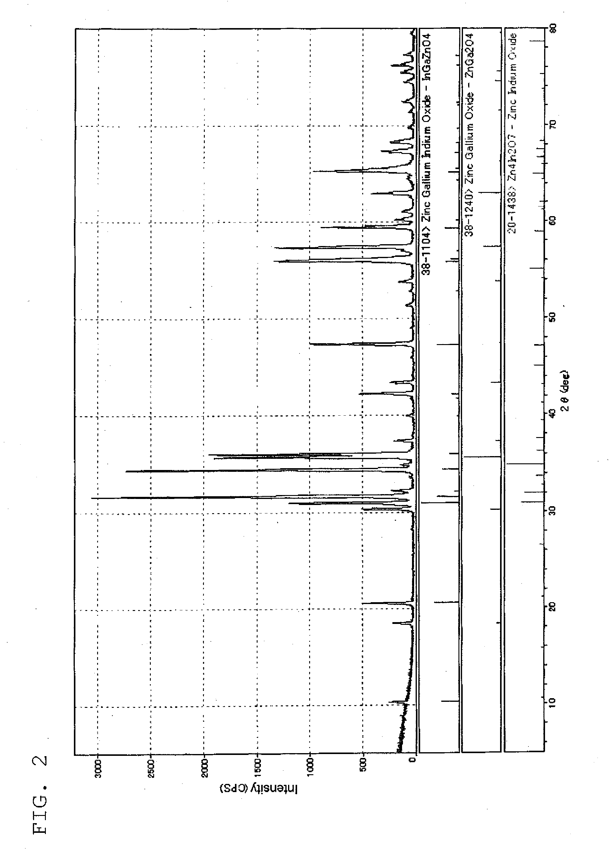
[0097]The sputtering target of the invention (hereinafter often referred to as the target of the invention) contains oxides of indium (In), gallium (Ga) and zinc (Zn), and comprises a homologous compound shown by InGaO3(ZnO)m (m is an integer of 1 to 20) and a spinel structure compound shown by ZnGa2O4.
[0098]The homologous compound is a compound having a homologous phase.
[0099]The homologous phase (Homologous Series) is, for example, a magneli phase shown by a compositional formula TinO2n-1, taking n as a natural number. In such a phase, there are a series of compounds in which n varies continuously.
[0100]Specific examples of the homologous compound include In2O3(ZnO)m (wherein m is an integer of 2 to 20), InGaO3(ZnO)m (wherein m is an integer of 2 to 20), or the like.
[0101]As described in “Crystal Chemistry” (Mitsuoki Nakahira, Kodansha, 1973) or the like, an AB2X4 type or an A2BX4 type is called a spinel structure, and a compound having such a crystal structure is generally called...
example 1
[0230]99.99%-pure indium oxide powder with a specific surface area of 6 m2 / g, 99.99%-pure gallium oxide powder with a specific surface area of 6 m2 / g, and 99.99%-pure zinc oxide powder with a specific surface area of 3 m2 / g were weighed such that the weight ratio of In2O3:Ga2O3:ZnO became 45:30:25. The powder was then subjected to mixing / pulverization by means of a wet medium stirring mill. As the medium of the wet medium stirring mill, zirconia beads with a diameter of 1 mm were used.
[0231]After the mixing / pulverization, the specific surface area of each raw material powder was increased by 2 m2 / g. The raw material powder was then dried by means of a spray dryer. The resulting mixed powder was placed in a mold, and then subject to pressure molding by means of a cold pressing machine, whereby a molded product was produced.
[0232]The resulting molded product was sintered for 4 hours at a high temperature of 1400° C. in an oxygen atmosphere by circulating oxygen. As a result, a sintere...
PUM
| Property | Measurement | Unit |
|---|---|---|
| Temperature | aaaaa | aaaaa |
| Temperature | aaaaa | aaaaa |
| Temperature | aaaaa | aaaaa |
Abstract
Description
Claims
Application Information