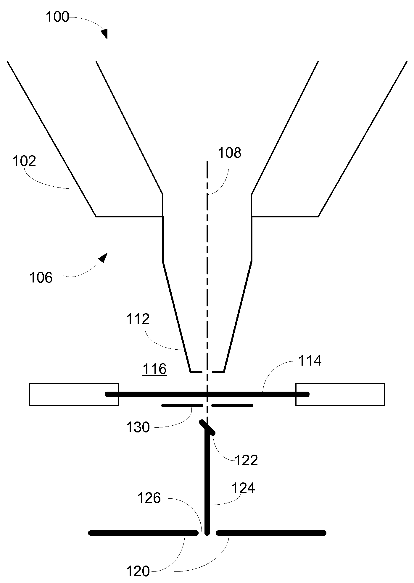
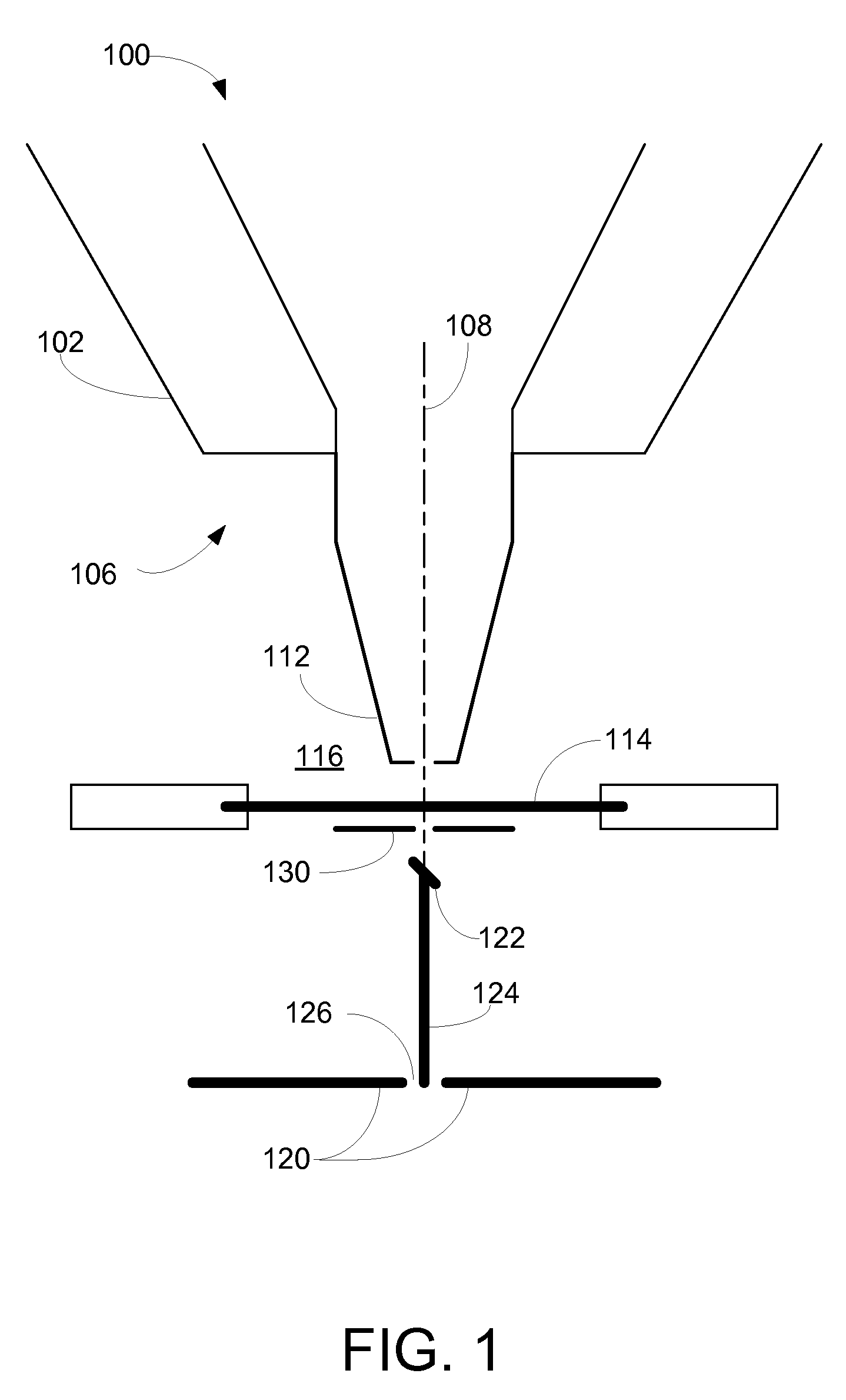
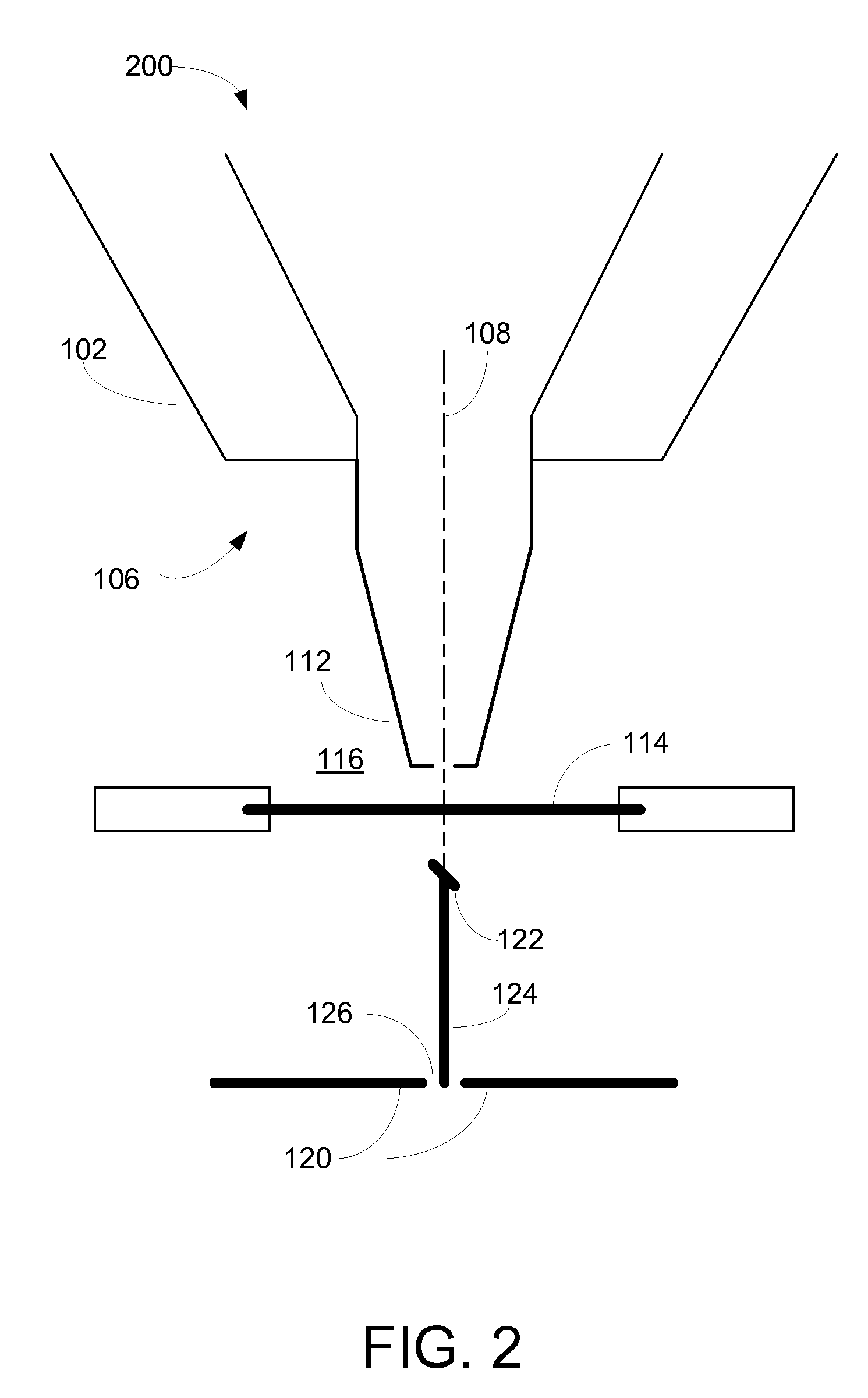
[0008]In an HPSEM, the sample that is to be investigated is placed in an
atmosphere of a gas having a pressure typically between 0.01
Torr (1.3 Pa) and 50
Torr (7000 Pa), and more typically between 1
Torr (130 Pa) and 10 Torr (1,300 Pa) whereas in a conventional SEM the sample is located typically in a vacuum of about 10−6 Torr (1.3×10⁻⁶ mbar). Unlike a conventional SEM, an HPSEM can readily form electron-optical images of moist or non-conducting samples, such as biological samples, plastics,
ceramic materials and glass fibers, which would be difficult to image under the typical vacuum conditions of a conventional SEM. The HPSEM allows samples to be maintained in their
natural state, without being subjected to the disadvantageous effects of
drying, freezing or
vacuum coating, which are normally necessary in studies of such samples using conventional SEMs. The
gaseous atmosphere of an HPSEM
sample chamber provides inherent charge
neutralization, that is, the dissipation of
surface charge that accumulates on a non-conductive sample as a result of
irradiation. Dissipating
surface charge increases resolving power of the
microscope.
[0009]The gas type used in an HPSEM can be selected so as to enable electron-beam induced chemical
processing of the sample. In such processes, electrons dissociate gas molecules adsorbed to the sample surface to produce reactive fragments that give rise to material deposition or volatilization in the vicinity of the electron beam. For example, Adachi et al. [Applied Surface Science 76, 11 (1994)] used CH4 to deposit carbon, Folch et al. [Applied
Physics Letters 66, 2080 (1995)] used Au(CH3)2(hexafluoroacetylacetonate) to deposit Au-containing nanocomposites, Ochiai et al., [Journal of Vacuum Science and Technology B 14, 3887 (1996)] used (HFA•Cu•VTMS) to deposit Cu-containing nanocomposites, Li et al. [Applied
Physics Letters 93, 023130 (2008)] used WF6 to deposit WO3-containing Nanocomposites, and Toth et al. [Journal of Applied
Physics 101, 054309 (2007)] used XeF2 to etch Cr.
[0010]Conventional scintillator-photomultipliers and solid state detectors can not be used for secondary electron imaging in a
gaseous atmosphere, because the detector bias needed to accelerate the low energy secondary electrons to the energy needed for efficient detector operation will cause
dielectric breakdown of the gas. An HPSEM, therefore, uses a different mode of detection, referred to as gas
cascade amplification. In gas
cascade amplification, a
voltage is applied between the sample surface and a
metal electrode (“
anode”). The liberated secondary electrons are accelerated toward the
anode and collide en
route with gas molecules in their path. These collisions will result in the liberation of new electrons, referred to as “
daughter electrons,” and gaseous ions from the gas molecules. The
daughter electrons and the ions will move towards and away from the
anode, respectively. In their turn, these newly liberated
daughter electrons will again collide with other gas molecules, and so forth, so that a cascade amplification of the secondary electron
signal occurs. The gas-cascade-amplified secondary electron
imaging signal is detected by measuring a current flow induced in electrodes such as the anode or the specimen holder, or by detecting photons generated by the gas cascade.
[0011]Combining a high pressure sample environment with an STEM presents difficulties. Conventional gas cascade amplification as used in a HPSEM will not produce adequate contrast in a STEM. The
image contrast of a STEM is derived from separately detecting either transmitted electrons that are scattered by the sample or transmitted electrons that are not scattered by the sample. The gas in a high pressure sample environment process, however, scatters the transmitted electrons, and thereby mixes the scattered and unscattered transmitted electron signals, impeding the formation of a useable image. In addition, gas cascade detectors measure the
signal induced in an
electrode by the motion of charge in the gas, or
luminescence generated by the gas cascade. Both of these signals are omnidirectional and serve to further mix the scattered and unscattered transmitted electron imaging signals, thereby impeding further the formation of a useful image.
[0012]Conventional scintillator-photomultiplier detectors are impractical for high pressure STEM because they are bulky and difficult to incorporate below a sample in a HPSEM chamber. Hence, solid state detectors are typically used for transmitted electron imaging in HPSEM systems. However, solid state detectors suffer from a number of problems. When imaging a wet sample, water droplets may fall on the detector below. Common samples include cross-sectioned
biological tissue and liquids suspended on perforated membranes, and often contain loose materials such as organic residue and nanoparticles. Such loose materials may be transported by the falling water droplets and may deposit on the detector surface. Because a
solid state detector requires electrons to strike the
depletion region with sufficient energy to excite the electron-hole pairs, any material on top of the detector reduces the number and energy of electrons reaching the depletion region, causing a loss of efficiency of the detector. For example, with just a micron of residue on the surface of the detector, a 30 kV electron might lose half its energy but still deposit 15 kV into the detector, but a 10 kV electron might lose all of its energy in the residue and not deposit any energy into the detector. Alternatively, a transmitted electron may be backscattered by the residue, and hence not deposit any energy into the depletion region. If a scintillator-photomultiplier detector is used in place of the
solid state detector, it will suffer from an analogous problem. A scintillator-photomultiplier detector requires electrons to strike the scintillator with sufficient energy to excite photons, and any material on top of the detector reduces the energy of electrons reaching the scintillator and the number of electrons reaching the scintillator, thereby lowering the number of photons generated per transmitted electron, causing a loss of detector efficiency.
Solid state detectors and scintillators are also fragile and difficult to clean.
[0013]Moreover, solid state detectors and scintillator-photomultiplier detectors are not compatible with some of the precursors used for electron-beam induced chemical
processing. Some such precursors are highly reactive, and some, like XeF2, may spontaneously etch detector components. Even if the detector were not spontaneously etched, the detector surface would be subjected to charged-particle-induced reactions as the sample, because the charged particles that are transmitted tough the sample
impact on the detector in the presence of the precursors. This problem is particularly severe in HPSEM systems where the precursor pressure at the detector surface is typically similar or equal to the precursor pressure at the sample surface.


